113 KiB
Write-up of FPGA Accelerator for StackSynth
- TODOs
- Reduce use of backticks
- Move large listings to appendix
- Measure SNR
- Move User Guide into appendix
- DS1881E-050+ Volume control???
Title Page
Standard Template is on Intranet
- Project Title: FPGA Accelerator for StackSynth
- Student: Aadi Desai
- CID: 01737164
- Course: EIE4
- Project Supervisor: Dr Edward Stott
- Second Marker: Dr Thomas J.W Clarke
Acknowledgements
I would like to thank Dr Ed Stott for his time and patience in the many meetings it took to discuss this project, as well as his guidance in architectural decisions that impacted the entire project. Without this insight, much more time may have been spend investigating alternatives and this project may not have reached a Proof-of-Concept stage that is useful for future students of the 3rd Year Embedded Systems module.
I would also like to thank my friends and family for their support and encouragement throughout the project, especially my peers who stayed up late with me as we worked on our projects together.
Abstract
The StackSynth module is an educational synthesiser platform based on the STM32L432, an ARM Cortex-M4 based CPU, which is well suited for the low-level realtime programming learning objective of the Embedded Systems module. However, it is not optimised for the Digital Signal Processing operations needed for complex audio waveform generation.
This project develops an FPGA-based extension module for StackSynth, with the purpose of increasing the audio ability and performance of the synthesiser, while offering future Embedded Systems students an opportunity to develop code for a RISC-V System-on-Chip. The main contribution of this project is the SystemVerilog modules and LiteX wrappers for receiving low-speed CAN frames, producing waveforms for a given frequency, converting from phase to a sine wave and driving the PCM1780 DAC audio / control ports. In addition, there are demo C++ programs and helper functions for interfacing with the custom logic and finally, integration of these custom logic blocks into a LiteX project that facilitates the use of the existing IP for the CPU, memory controller, USB controller and serial interfaces.
The API for controlling the custom SystemVerilog logic has been designed to be simple to implement within student-written FreeRTOS tasks, similar to the existing Embedded Systems Module coursework C++ architecture.
Contents
- Title Page
- Acknowledgements
- Abstract
- Contents
- List of Figures
- List of Listings
- List of Tables
- List of Abbreviations
- Introduction
- Background
- Analysis and Design
- Implementation
- Testing and Results
- Evaluation
- Conclusions and Further Work
- User Guide
- Bibliography
- Appendix
List of Figures
TODO
List of Listings
TODO
List of Tables
TODO
List of Abbreviations
- ACM: Abstract Control Model (USB Class)
- AXI: Advanced eXtensible Interface
- BRAM: Block RAM
- CAN: Controller Area Network
- CDC: Communications Device Class (USB Class)
- CPU: Central Processing Unit
- CSR: Control and Status Register
- DAC: Digital-to-Analogue Converter
- DFU: Device Firmware Upgrade (USB Class)
- DSL: Domain Specific Language
- DUT: Device Under Test
- FIFO: First-In First-Out
- FPGA: Field-Programmable Gate Array
- GPIO: General Purpose Input/Output
- GUI: Graphical User Interface
- HDL: Hardware Description Language
- IRQ: Interrupt ReQuest
- ISR: Interrupt Service Routine
- LSB: Least Significant Bit
- LUT: Look-Up Table
- MOSFET: Metal-Oxide Semiconductor Field-Effect Transistor
- MSB: Most Significant Bit
- PLL: Phase-Locked Loop
- PWM: Pulse-Width Modulation
- QSPI: Quad Serial Peripheral Interface
- RAM: Random Access Memory
- ROM: Read-Only Memory
- RTL: Register-Transfer Level
- SoC: System-on-Chip
- TTY: TeleTYpe (USB Class)
- VCD: Value Change Dump
Introduction
The 3rd Year Embedded Systems course of the Electrical Engineering department at Imperial College London includes a coursework designed to teach students real-time programming in a resource constrained system. The scenario of the coursework is a music synthesiser where audio samples must be generated consistently to ensure audio without glitches.
This project aims to extend the capabilities and performance of the existing educational platform as the microcontroller currently used in the coursework is limited to a small number of oscillators and basic audio effects. A key factor in the success of this project is that a student should be able to interact with the provided gateware in a similar manner to the existing coursework.
This project provides code for the gateware needed to run user-written programs, receive communications from CAN protocol devices and produce audio waveforms consisting of 64 individual waves of specified frequencies, as well as demonstration software to control the provided gateware via CAN frames or direct control via a console interface.
Report Structure
The report is structured as follows:
- Chapter 2 - Background - Determines the project base and goals, and introduces aspects of the project that are pre-determined, including the FPGA used and external components present on the StackSynth Extension board
- Chapter 3 - Analysis and Design - Lays out the architecture of the system and connections between modules
- Chapter 4 - Implementation - Details the design decisions made during development and features of the project as completed
- Chapter 5 - Testing and Results - Covers testing throughout the project used to verify functional correctness of the design and measure performance
- Chapter 6 - Evaluation - Evaluates the project on progress against the identified objectives and areas that can be improved
- Chapter 7 - Conclusions - Concludes the project, including insights into future work
Background
This section goes over the research and existing work that this project builds upon, as well as key aspects of the project that inform the analysis and design stages. The sub-sections focus on the StackSynth module, OrangeCrab board, LiteX framework, PCM1780 DAC, CAN bus and ATA6561 transceiver.
Requirements Capture
The aim of this project is to extend the existing StackSynth platform that is used in the 3rd Year Embedded Systems (ELEC60013) with an FPGA accelerator to increase the audio performance and capabilities of the StackSynth educational platform. The key motivators are to allow for many more oscillators than is possible on the ST Nucleo L432KC as well as advanced effects such as equalisation with multiple filter taps, as the available time for generating samples on the L432KC is limited due to strict deadlines for sample timing to prevent audible glitches.
The original brief mentions that using an FPGA would allow for "hundreds" of simultaneous oscillators and filter taps, however the maximum number of oscillators and filter taps is likely to be limited by the available logic on the FPGA fabric, as the selected model of FPGA has 24,000 LUTs (look-up tables) to create logic blocks from. This is discussed later in the FPGA Utilisation section. The brief also states that "a professional-grade sample rate and resolution" should be achievable, so the industry standard for "CD-quality" is used as a baseline giving a target of 16-bit 44.1kHz output, as higher bit depth and sampling rate is often not perceived.
As the end goal is to have an educational aid, there are some quantitative targets for usability. Using the FPGA accelerator should be an extension of the existing coursework, with difficulty caused by intentional complexity of the project, not from implementation details that cannot be changed by the student. The syllabus for the embedded systems module [ELEC60013] states learning objective including: low-level communication, real-time constraint analysis, interrupts and multi-threading. The FPGA extension will allow students to program an embedded SoC and develop code to communicate with the main StackSynth boards, using interrupt service routines and handlers.
The embedded SoC will run student developed code which handles various tasks including: communication with other StackSynth modules via the CAN bus, controlling the oscillators and filter taps and processing of slower loops such as low-frequency oscillators and other effects over longer periods of time. The digital logic blocks to be developed in this project are the CAN receiver, sample generator and blocks to drive the various buses to control the onboard DAC and amplifier.
The core contributions of this project are the following:
- Quarter-wave sine wave approximation CORDIC SystemVerilog module and multi-wave generator LiteX module
- PCM1780 Audio driver and Mode Control SystemVerilog and LiteX modules
- CAN receiver SystemVerilog and LiteX module, used to receive and acknowledge CAN frames from StackSynth boards
- LiteX project including hardware interrupts, which can be used as a base for further development
- Demo code including programs and helper functions for interacting with custom modules from software
StackSynth Board
The StackSynth board is part of an educational platform designed to teach real-time programming in the situation of a music synthesiser, and is part of the 3rd Year Embedded Systems [ELEC60013] module. It utilises the PlatformIO framework which provides the HAL (Hardware Abstraction Layer) and a port of the Arduino Framework (Stm32duino) which allows for easier control of external pins of the microcontroller.
A music synthesizer is a good demonstration of real-time programming and prioritisation of work, as latency in an audio stream is less important than interval consistency of audio samples, resulting in strict deadlines for sample generation. The StackSynth board uses a Nucleo STM32L432KC board (datasheet), which has an ARM Cortex-M4 core, as well as 11 timers with varying precision and uses, and direct support for the CAN protocol in the provided HAL as detailed in section 3.29 of the [datasheet]. The timers are especially helpful for setting task interval initiation interrupts, pre-empting lower priority tasks so that deadlines are not missed.
The ARM Cortex-M4 core has support for some DSP (digital signal processing) instructions, as defined in Table 3-2, ARM Cortex-M4 DSP Instructions, however these are not optimised for operating on many samples in parallel or for the complex DSP operations of an equaliser filter tap. FPGA logic operates simultaneously each clock cycle, so can operate on every sample at once in a pipeline reducing the latency of audio effects.
Communication on the CAN bus will still be done on the StackSynth module, including notedown and noteup events, defined by sending P or R in byte 0 of the CAN frame respectively, in addition to student-defined messages such as waveform and filter settings if controlled from a StackSynth module.
StackSynth FPGA Extension Board
Audio sample generation is subsequently handled on the FPGA extension board where students will decode their CAN messages on the embedded SoC and then control the oscillators and filters. The extension board has headers for attaching the OrangeCrab FPGA module and a few chips along with passive components for tasks not handled within the FPGA.
A Microchip ATA6561 CAN Transceiver along with connectors along the sides of the board allow for detection of and communication with other StackSynth modules via the CAN bus. The transceiver handles conversion from high and low logic states to recessive and dominant states on the CANH and CANL pins, and is discussed in more detail in a later section.
A Texas Instruments PCM1780 DAC is connected to the FPGA GPIO pins, with the output connected to one 3.5mm headphone port and the input of an Analog Devices DS1881E-050+ (datasheet) digital potentiometer which is used to adjust the amplitude of the analogue waveform providing volume control. This waveform is the input to a TS482IST (datasheet) 100mW stereo amplifier which provides enough amplification and power to drive low impedance speakers and headphones via a second 3.5mm headphone port.
OrangeCrab Board
The OrangeCrab is a development board built around the LFE5U-25F and LFE5U-85F, which are part of the Lattice Semiconductor ECP5 family of FPGAs. For this project, the LFE5U-25F model of the OrangeCrab was used due to limited availability and increased cost of the larger FPGA model. The specifications of the LFE5U-25F are as follows: 24,000 LUTs, 1008Kb of embedded Block RAM, 194kb of distributed RAM, 28 18-bit multipliers and 2 PLLs. The OrangeCrab also includes 128Mb of non-volatile QSPI flash used for storing the bootloader/bitstreams/user-firmware, a MicroSD card slot and a 48MHz oscillator used as a source for the system-clock PLL.
The OrangeCrab follows the Adafruit Feather form factor, making it physically compatible with FeatherWings which are stackable expansion boards for Feather boards. This means the OrangeCrab could be swapped out for a more powerful board using the same pin layout if required in the future. Various FPGA pins are routed to the external pins of the board, allowing for direct connections from a design to external devices, which will be used in this project to communicate with the ATA6561 CAN Transceiver, PCM1780 DAC and TS482IST digital potentiometer.
The OrangeCrab hardware is released as open-source under the CERN Open Hardware Licence v1.2, along with firmware released under the MIT Licence in the GitHub Repository. Bitstreams for flashing the FPGA can be created with either Lattice Semiconductor's Diamond IDE or the open-source Project Trellis toolchain which uses Yosys for synthesis and nextpnr for placement and routing. Gateware and software examples are also provided in another GitHub Repository.
The r0.2.1 board also features a USB-C port connected directly to pins on the FPGA, allowing a design to present itself to USB hosts as a DFU (Device Firmware Upgrade), TTY (Teletype), CDC (Communications Device Class), ACM (Abstract Control Model) or even a composite USB device. Along with the pre-flashed bootloader, which presents a DFU endpoint, the OrangeCrab can be flashed without an external programmer.
The USB port operates at USB 2.0 Full Speed (12Mbps) as higher speeds are not possible on the ECP5. It can be used in user designs by instantiating a USB core, and the demo program uses ValentyUSB, enumerating as a CDC-ACM device, which results in a COM port on Windows and /dev/ttyACMx on Linux.
LiteX Framework
LiteX is a framework for creating FPGA cores and complex SoCs, using many provided cores such as CPUs, DRAM interfaces and protocol buses, eg Wishbone, AXI, Avalon. LiteX is used in this project as it provides many useful cores and makes connecting different blocks together easier, reducing the time taken for this project to reach a working Proof of Concept.
LiteX has support for a large range of boards, and the creator of the OrangeCrab added support in litex-hub/litex-boards, PR #59, including the necessary pin definitions and Project Trellis toolchain steps for creating the bitstream for the OrangeCrab r0.2(.1) used in this project with Yosys and nextpnr targetting the Lattice Semiconductor ECP5.
The LiteX project initially built upon Migen (homepage), so many of the Migen cores are still available and the overall method of defining modules, synchronous and combinatorial logic remains in line with Migen. Migen - and by extension LiteX - is a DSL (Domain Specific Language) using Python and the dictionary nature of all variables to provide terse syntax for defining logic. This syntax is shown in Listing x.y [below].
[Listing: Example of defining comb and sync logic in LiteX]
self.delay = Signal()
self.delay1 = Signal()
self.comb += self.delay1.eq(self.delay + 1)
self.sync += self.delay.eq(self.delay1)
After defining logic and instantiating blocks within a design, the provided Builder() function iterates through the map of the defined BaseSoC object and converts the design to a Verilog file representing the full design. The resulting Verilog file has ports for connections to external pins, defined in the Pin Constraints File, and is synthesised using Yosys, along with any SystemVerilog and Verilog files instantiated within the design using the Instance() function. An example of this is shown in Listing x.y [below], taken from modules/testPropagation.py where the saw2sin module is instantiated.
[Listing: Example of Instance() function]
self.i_saw = Signal(16)
self.o_sin = Signal(16)
self.specials += Instance("saw2sin",
    i_i_clk = ClockSignal(),
    i_i_saw = self.i_saw,
    o_o_sin = self.o_sin,
)
The key components of LiteX used in this project are:
GSD_OrangeCrab.Platform: defines connections from external FPGA pins to peripherals, eg. the QSPI flash, DDR3L RAM and board GPIO, as well as required blocks such as clock sources, PLLs, the CPU and the USB PHY for serial communicationClockDomain: creates a new clock domain, used for the DAC system clock, driven at 36.864MHz as indicated in the PCM1780 datasheet for a 48kHz sample rateSubsignal: defines collections of signals for easier pin assignment within modulesLiteScopeAnalyzer: a logic analyser placed alongside the SoC, sampling any selected signals within the design at the system clock frequency, with values stored in Block RAM and converted a VCD waveform file which can be viewed in GTKWaveBuilder: converts the design object to a Verilog module and invokes Yosys and nextpnr to synthesize and generate the FPGA bitstreamModule: creates a custom module that can be instanced and added as a submodule to other modules or theBaseSoCModuleDoc: inheriting from this class results in the class docstring being used in the autogenerated documentation, allowing the documentation of a module to be placed alongside the module definitionCSRStorage: register object that is read/write from the CPU and read-only from custom logicCSRStatus: register object that is read-only from the CPU and driven from custom logicAutoCSR: inheriting from this class adds all detectedCSRStorageandCSRStatusblocks within a module to the CSR bus, providing preprocessor definitions for register addresses as well as functions to read/write to the registers or individual fields within the registersInstance: creates an instance of an external Verilog or SystemVerilog module, including connections from the module ports to the LiteX designAsyncFIFO: core from the Migen library with read and write ports that can be located in different clock domains. Grey code is used to prevent metastability issues in the full and empty flags. It is used to transfer generated samples from the system clock domain at 48MHz to the DAC clock domain at 36.864MHz
PCM1780 DAC
The PCM1780 is a 2 channel DAC supporting 16-24bit samples at a 8-192kHz sampling frequency. Audio samples can be input via I2S, right-justified or left-justified formats, and separate buses are used for transferring audio samples or controlling the mode settings of the DAC. The PCM1780 is used in this project to provide superior audio quality than other methods of outputting audio from the FPGA, such as PWM (Pulse Width Modulation).
The PCM1780 settings are controlled via a 3-wire SPI-like interface, with a chip-select, clock and data-in pin. No data is ever read from the DAC so the data-out pin is not present. The available settings are shown in Table x.y [below], taken from [Table 5. User-Programmable Mode Controls] of the datasheet.
[Table: PCM1780 settings]
| Function | Reset Default | Register | Bit(s) |
|---|---|---|---|
| Digital attenuation control | 0 dB, no attenuation | 16 + 17 | AT1[7:0], AT2[7:0] |
| Soft mute control | Mute disabled | 18 | MUT[2:0] |
| Oversampling rate control | ×64, ×32, ×16 | 18 | OVER |
| Soft reset control | Reset disabled | 18 | SRST |
| DAC operation control | DAC1 and DAC2 enabled | 19 | DAC[2:1] |
| De-emphasis function control | De-emphasis disabled | 19 | DM12 |
| De-emphasis sample rate selection | 44.1 kHz | 19 | DMF[1:0] |
| Audio data format control | 24-bit, left-justified | 20 | FMT[2:0] |
| Digital filter rolloff control | Sharp rolloff | 20 | FLT |
| Digital attenuation mode select | 0 to –63 dB, 0.5 dB/step | 21 | DAMS |
| Output phase select | Normal Phase | 22 | DREV |
| Zero-flag polarity select | High | 22 | ZREV |
| Zero-flag function select | L-, R-channels independent | 22 | AZRO |
The default settings for the PCM1780 are ideal for this project, though the digital attenuation may be used as another point of volume control, possibly to normalise the output volume regardless of the number of oscillators that are active. As such the only settings that need to be modified are the attenuation level for the left and right channels.
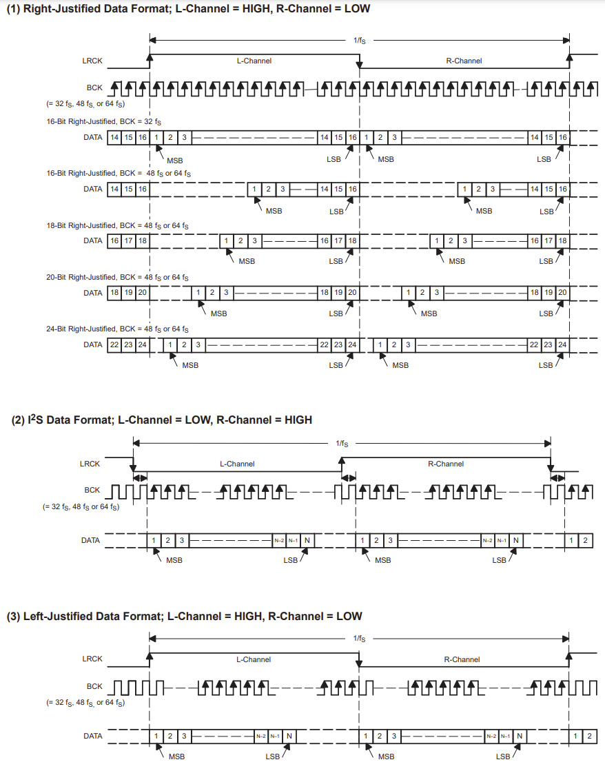
The default settings also include the audio sample format of left-justified, which allows for flexibility of the sample depth as a 16-bit sample is equivalent to a 24-bit sample where the low 8 bits are 0. To give this output, a shift register can be used to output the sample bit by bit, updated on the falling edge of the bit clock as shown in Appendix x.y, taken from [Figure 22. Audio Data Input Formats] of the datasheet. The bit clock can run at 32x, 48x or 64x the sampling frequency and can be selected for easier implementation within the SystemVerilog design, though the bit depth is limited by lower bit clock frequencies.
- TODO: move to appendix
[Figure: PCM1780 audio data input formats]
The timing diagram of the control interface is shown in Figure x.y [below], taken from [Figure 26. Control Interface Timing] of the datasheet. In the figure, MC pulse cycle time limits the maximum frequency of the clock signal, and the value of 100ns results in a maximum frequency of 10MHz. As the OrangeCrab has a 48MHz system clock, a 6MHz clock signal can be generated using a 1:8 clock divider, simplifying the design and reducing delay / clock skew. The timing diagram also shows setup and hold time requirements for the data signal.
[Figure: PCM1780 control interface timing diagram]
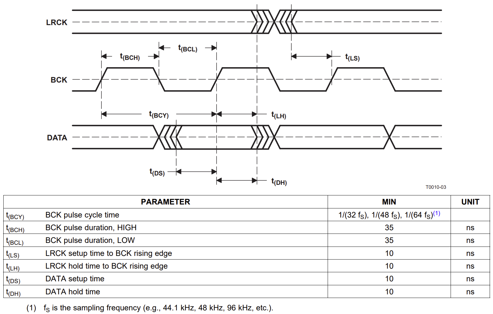
The data to be sent will be crossing from a 48MHz clock domain into a 6MHz clock domain, but as the latter is derived from the former using logic, there is no risk of a change in phase and metastability can be avoided by holding the value stable in the faster domain for multiple clock cycles and buffering the value in the slower domain. In this design, the value can be left constant until a new value is set as the action of setting the attenuation value is idempotent and does not have a side-effect from being repeated.
CAN Bus
The CAN (Controller Area Network) bus is a differential serial bus used for communication between devices, typically in automotive applications due to its ability to withstand electromagnetic interference and wiring simplicity requiring only a twisted pair of wires common to all devices on the bus. The Wikipedia page for the CAN bus provides an overview including key features of the protocol, however for timing and implementation specifics, the Bosch CAN Specification 2.0 and Texas Instruments: Introduction to CAN documents were used as reference material.
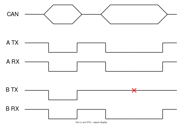
The CAN bus is a multi-master bus, so any device can transmit at any time. In order to prevent collisions and loss of data, a form of arbitration is used to select which device has priority. This is done by assigning each message a unique ID, and the device with the lowest ID wins arbitration. This is inherent to the design of the CAN bus as transmitting a 0 is done by asserting the dominant state on the CANH and CANL signals and each device measures the state of the bus to determine if it should stop transmitting, so a device transmitting a recessive state will still be able to detect the dominant state. This is shown in Figure x.y [below], where device A uses a lower ID than device B and so device B stops transmitting when it detects the dominant state on the bus at the red cross.
[Figure: CAN bus arbitration]
In this project, low-speed CAN is used as the data to be transferred between devices is a few bytes at a time, and limited by the student code on each StackSynth module. In addition, the length of the CAN bus is determined by how many StackSynth devices are chained together, resulting in ~15cm per module so electromagnetic interference is unlikely to be an issue. On the StackSynth FPGA Extension board, the CAN bus signalling is handled by a Microchip ATA6561 Transceiver, as detailed in the following section.
Two key features of low-speed CAN are: a bit rate of 125k baud, resulting in ~8us per bit for propagation and sampling across the bus or 384 cycles at the 48MHz system clock of the OrangeCrab; and differential signalling, where the exact voltage levels of CANH and CANL are not important, but the polarity of the difference between the two signals (CANH - CANL) is used to determine the state of the bus, further reducing the impact of electromagnetic interference.
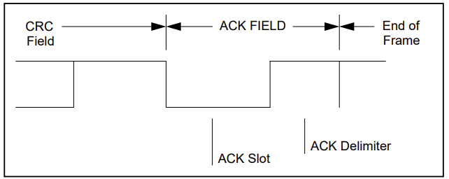
An important requirement of all CAN variants is that each frame must be acknowledged by at least one other device on the bus, otherwise the transmitting device may choose to retransmit the frame indefinitely or enter an error state. In the case of the StackSynth module, this results in the user-program CAN transmit queue being full, and the program blocking when attempting to add a new transmit message to the queue. The ATA6561 Transceiver does not contain any logic for automatically acknowledging frames, so the ACK signal must be generated within the FPGA logic. This is done by checking the ID of the received frame against a CAN receive ID filter after masking with a filter ID mask, and then driving the bus to a dominant state during the ACK bit of the frame if the frame is valid. Figure x.y, from "Section 3.1.1 Data Frame" of the Bosch CAN Specification 2.0 document, shows the ACK slot where a receiver transmits a dominant state overriding the transmitters recessive state.
[Figure: CAN frame format of ACK field]
The CAN Specification also indicates that the bus should be sampled at 75% of the "bit time", or 6us into a bit for a 8us period in low-speed CAN. This precise timing is maintained by synchronising every device on the CAN bus with each incoming recessive to dominant transmission. This occurs at the start of each frame as well as throughout the frame, at least as often as every 10 bits due to the presence of stuffed bits, preventing a build-up of clock skew and errors in sampled bits.
The CAN protocol is a NRZ (Non Return-to-Zero) protocol, meaning consecutive bits of the same polarity result in no change in the bus state. If many consecutive bits of the same polarity were transmitted, this could result in devices losing synchronisation with each other if there were differences in internal clock frequencies and timing. To prevent this, bit stuffing is used, where extra bits of opposing polarity are added after a sequence of consecutive bits of the same polarity, with stuffed bits counting towards the sequence of consecutive bits. In CAN, a stuffed bit is added after 5 consecutive bits of the same polarity, so a stuffed bit can occur after every 4 non-stuffed bits. This is shown in Listing x.y [below], where a sequence of 10 bits is stuffed to a length of 12 bits, with the 6th and 11th bits being stuffed bits indicated in red. An error occurs on the CAN bus if 6 consecutive bits of the same polarity are detected, with the exception of the End-Of-Frame marker which has no stuffed bits and is always 7 consecutive 1s.
[Listing: Bit stuffing example]
0000011110 \rightarrow 00000{red}{1}1111{red}{0}0
A complete CAN bus frame is shown in Figure x.y, from the Wikipedia page on the CAN bus, where the frame ID is 0x14 and the frame contains 1 byte of data. In the case of the StackSynth module, the data length is hardcoded to 8 bytes within the CAN helper library, with unused bytes being ignored by the receiving device.
[Figure: CAN frame format]
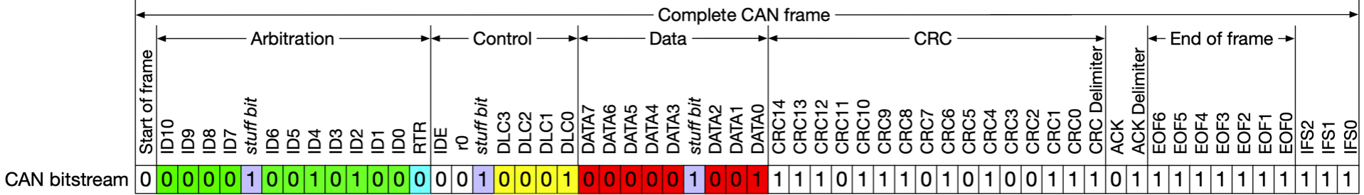
In addition to the frame ID, data length and data bytes, the CAN frame also contains a CRC (Cyclic Redundancy Check) field which allows for detection of errors in the received frame. This is calculated using the generator polynomial x^15+x^14+x^10+x^8+x^7+x^4+x^3+1 as prescribed in the Bosch CAN Specification 2.0 with the input sequence of the Start-Of-Frame, Frame ID, Control Field (ID extension bit, reserved bit and data length code) and Data Field. As described in the CAN specification, this can be implemented using a shift register with an XOR with 0x4599 when the next incoming bit is high. The CRC is then transmitted in the CRC field of the CAN frame, and the receiving device can calculate the CRC of the received frame and compare it to the received CRC to determine if the frame is valid. If the CRC is not valid, the frame is discarded and the receiving device does not acknowledge the frame.
ATA6561 CAN Transceiver
The Microchip ATA6561 (datasheet) is a CAN and CAN-FD capable Transceiver chip that provides a physical interface from a CAN protocol controller to the CANH and CANL pins as well as protection against ESD and other faults on the CAN bus such as electrical short-circuits that could occur when (dis-)connecting StackSynth modules. It is used to convert CAN protocol bits from the FPGA to differential signals required on the CAN bus, and includes support for 3.3/5V tolerant inputs and outputs, allowing direct connections to microcontroller or FPGA external pins without level shifting. This direct connection is possible due to the STBY and TXD inputs being connected to the VIO pin via internal pull-up resistors and the RXD output being driven from VIO via a pair of MOSFETs as shown in Figure x.y [below], taken the Functional Block Diagram on page 3 of the ATA6561 [datasheet].
[Figure: ATA6561 Functional Block Diagram]
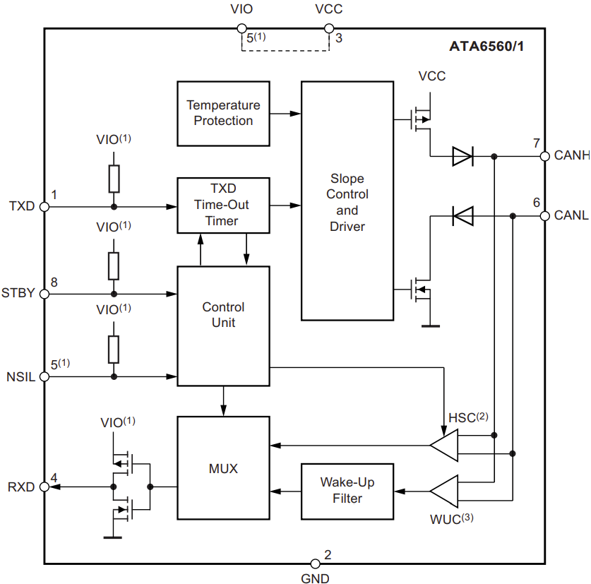
The ATA6561 also provides protection to the CAN bus from the CAN controller in two key situations. First, if the RXD pin is driven high externally, such as an accidental logic-high output from the FPGA or a short-circuit to VCC, this represents a recessive state and would prevent a CAN controller from detecting a dominant state on the CAN bus, causing arbitration to fail. Second, if the TXD pin is driven low for longer than the TXD dominant timeout, the CANH and CANL pins are disconnected (high-impedance) as driving a constant dominant state on the CAN bus would block all other network communication. This timeout is reset when the TXD pin is driven to logic-high.
The transceiver has 4 operating modes, however only Normal mode is used, as this allows for monitoring of the CAN bus via the RXD pin, and driving the CAN bus to the dominant state when TXD is driven low, such as for acknowledging a received frame. The other modes are Unpowered, Standby and Silent, which are either not useful in operation, or in the case of Silent, is not accessible on the ATA6561 by the user, and only occurs when an error is detected on the CAN bus. Finally, the ATA6561 is a clockless and combinatorial device, and can be treated as a direct connection from the FPGA to the CAN bus. The FPGA logic keeps track of bit timing, and drives the TXD pin as needed.
Analysis and Design
This section presents a high-level overview of the design of the system, and details design decisions that apply to the system as a whole rather than a specific area of implementation. Changes that were made to the design during implementation are discussed in the implementation section.
Figure x.y [below] is a block diagram representation of the StackSynth FPGA Extension board including SoC and external Integrated Circuit components that are integral to the project function. Dotted lines represent analogue signals, which includes the stereo audio signals from the PCM1780 DAC, through the DS1881E digital potentiometer and through the TS482 amplifier and 3.5mm headphone port. Thinner solid lines are single bit digital signals, including clock signals and serial bit connections, while thicker solid lines are multi-bit digital signals or buses, including UART and the CSR bus. Later in the project, the VexRiscV CPU was replaced with a PicoRV32 CPU for testing a basic software implementation of interrupts, however the overall architecture of the system remained unchanged.
The block diagram is also colour coded to represent the different areas of the system, with physical components confirmed at the start of the project in red, parts of the OrangeCrab in orange, LiteX provided modules on the FPGA in blue, and modules created in this project in green. The FTDI USB to UART adapter is shown in the diagram as it is used to download traces from the LiteScope Analyzer, however it was not provided as part of the project and is external to the StackSynth FPGA Extension board.
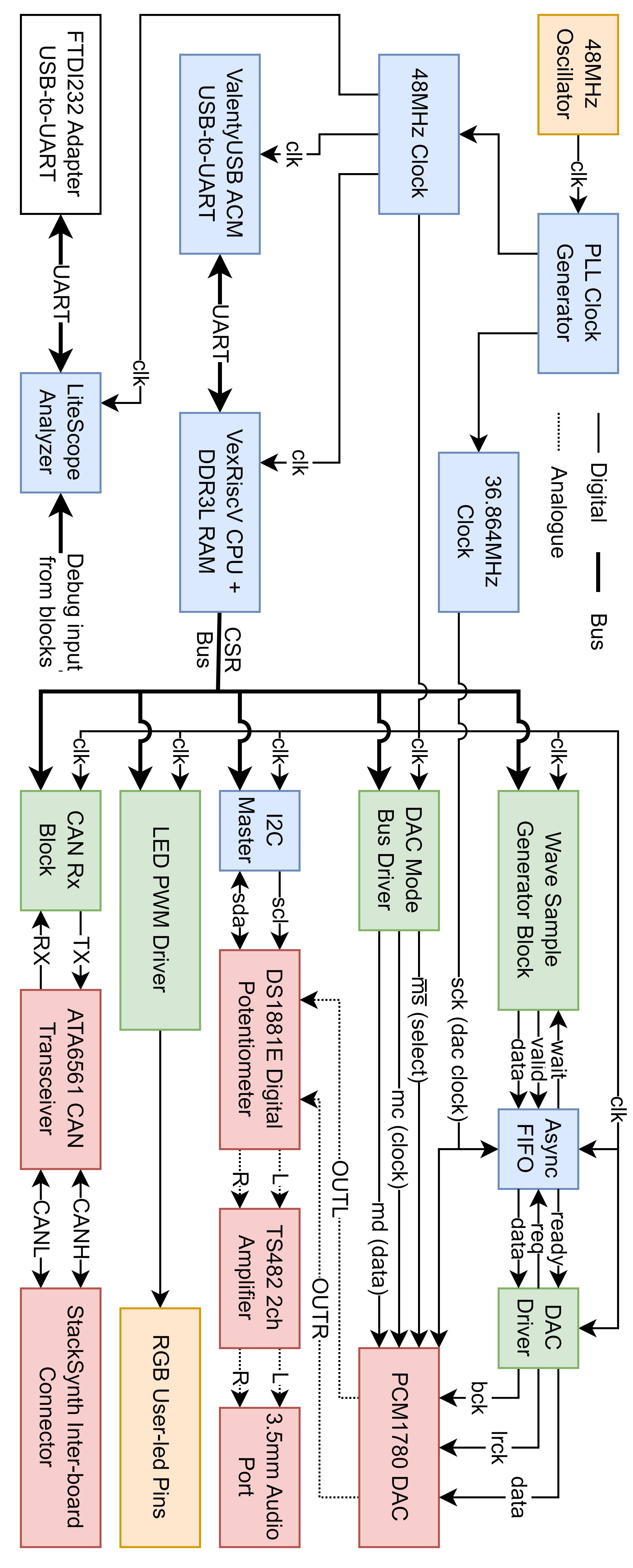
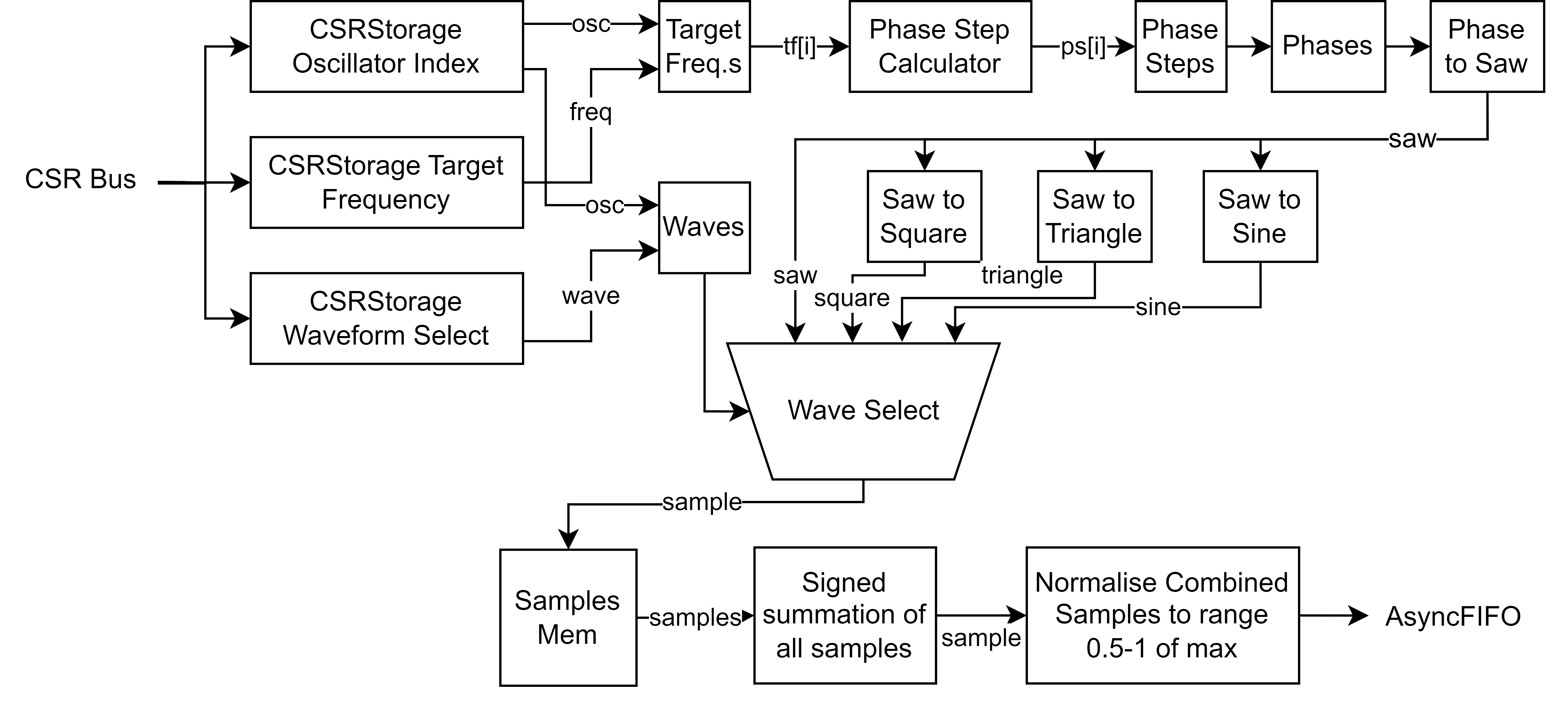
In Figure x.y, the Wave Sample Generator Block represents a conversion from settings controlled from the CPU via the CSR bus to the final output samples sent to the DAC. A key design decision within this block is the generation of sample values when required without the use of a large wave-table. The OrangeCrab has limited Block RAM and a large memory would be required to provide the resolution desired for phase to sine wave conversion, for example, using a 16-bit phase to index a table with 2^16 or 65536 entries would require 1049Kb of Block RAM, more than the 1008Kb available on the ECP5 model used. Instead, a larger phase accumulator can be used, allowing for more precise phase steps providing better accuracy as the error is smaller, and minor errors due to rounding are averaged out over multiple cycles, reducing the likelihood of audible glitches. This phase accumulator can then be truncated to 16 bits by ignoring the lower 8 bits and used for sample generation. Figure x.z shows the submodules within the Wave Sample Generator Block, including the CORDIC and GenerateWave modules.
[Figure: Wave Sample Generator Block internals]
The Async FIFO block handles the transfer of generated samples from the system 48MHz clock domain to the 36.864MHz DAC clock domain, as the write port is driven by the system clock and the read port is driven by the DAC clock. This block is required as the DAC clock is not a multiple of the system clock, nor does it divide from the system clock, so multiple buffers may not prevent metastability. The samples are then fed into the DAC Driver which uses an internal counter to generate the bit clock at 2.304MHz and left-right clock at 48kHz.
The final major design choice in this project is to use SystemVerilog (IEEE 1800-2017), including constructs such as always_comb and always_ff blocks over Verilog always blocks and logic over wire or reg. This choice was made for a number of reasons, including the extra compile time checks and readability as the block is immediately identifiable as combinatorial or synchronous logic and the ability to use newer open source tools for checking code quality and semantic correctness when writing the required blocks for logic not already provided by LiteX. However, the SystemVerilog constructs supported by the open-source version of Yosys used in Project Trellis are limited, so the code must still be written so that it can be synthesised by Yosys.
The first tool used is svlint, a SystemVerilog linter that provides a large range of syntax and style rules with the goal of improving code readability and maintainability, including rules to reduce simulation and synthesis errors due to mismatches in intent and implementation. The VSCode extension svlint-vscode is a language server client and communicates with svls, a language server built around svlint, providing compatibility with the Language Server Protocol and allowing for in-editor syntax highlighting and linting.
The second tool used is slang, a SystemVerilog parser and compiler with comprehensive support for the IEEE 1800-2017 SystemVerilog syntax. This tool is used to check for syntax errors in the SystemVerilog code as well as semantic errors such as mismatches in signal widths and types or invalid variable names including suggestions based on existing signals in the current file. An online version is available, with an editor on the left and a live compiler output on the right, however the tool can also be compiled and used offline.
Implementation
This section details the implementation of the project, with sub-sections covering different areas of the final implementation. These sub-sections do not represent the order of implementation, but rather logical grouping to keep relevant decision and design aspects together. Areas for further work are also briefly discussed, with further detail in the Further Work section. The implementation is available in the GitHub repository: supleed2/EIE4-FYP.
Setting up the LiteX Framework
As this project is built using the LiteX Framework, the project implementation begins with setting up the framework and creating a basic SoC including a custom module and connections from the CPU to the module so that the module can be controlled from software running on the CPU. A LiteX project consists of a main Python script that creates a class instance representing the SoC to be built including all peripherals and sub-modules, make.py in this project. This file is based on the gsd_orangecrab.py target file from the litex-boards GitHub repository, with modifications made to add the custom modules created as part of this project and debugging tools such as the LiteScope Analyzer. The build script uses the OrangeCrab platform class, which defaults to a VexRiscV-Standard CPU as the SoC core, but can be overridden from the command line with the --cpu-type and --cpu-variant flags.
An initial test of custom module creation was performed by replacing the LiteX-provided LedChaser with a custom module that reads a value set from a CSR and outputs the 3 PWM signals for the red, green and blue pins of the user_led (LED on the OrangeCrab). The TestRgb module creates a SCRStorage memory representing the target RGB value for the LED in 24 bit colour, and this register is connected to an input of the ledPwm SystemVerilog module where an 8 bit counter increments at the 48MHz system clock and the output is high if the target value is greater than the counter value for each LED channel. The three output pins are then connected using a comb statement to the LED pin objects within the LiteX module, and the SystemVerilog source file is added to the list of sources provided to Yosys for synthesis. The LiteX and SystemVerilog modules are included in Listing x.y and Listing x.z respectively for reference.
class TestRgb(Module, AutoCSR, ModuleDoc):
    """
    RGB LED Test Module
    """
    def __init__(self, platform, pads):
        self.pads = pads
        self._out = CSRStorage(size = 24, description="Led Output(s) Value (24-bit RGB)",
        fields = [
            CSRField("ledb", size = 8, description = "LED Blue Brightness"),
            CSRField("ledg", size = 8, description = "LED Green Brightness"),
            CSRField("ledr", size = 8, description = "LED Red Brightness"),
        ])

        # # #

        leds = Signal(3)
        self.comb += pads.eq(~leds)
        self.specials += Instance("ledPwm",
            i_clk = ClockSignal(),
            i_rgb = self._out.storage,
            o_ledr = leds[0],
            o_ledg = leds[1],
            o_ledb = leds[2]
        )
        platform.add_source("rtl/ledPwm.sv")
Listing: ledPwm SystemVerilog Module
`default_nettype none

module ledPwm
( input  var        clk
, input  var [23:0] rgb
, output var        ledr
, output var        ledg
, output var        ledb
);

logic [7:0] counter;

always_ff @(posedge clk)
  counter <= counter + 1;

always_comb ledr = (rgb[23:16] > counter);
always_comb ledg = (rgb[15: 8] > counter);
always_comb ledb = (rgb[ 7: 0] > counter);

endmodule
To test this module, the generated functions in generated/csr.h of the build output directory provide convenient functions for reading from and writing to CSR locations. The demo program has a function void leds_cmd(char** val) which allows the value of the CSR to be updated from the Serial Console that is accessible when the OrangeCrab is connected to a computer via USB. While testing this module resulted in immediately noticeable changes in the output colour of the LED, adding a reset pin caused the design to stop working, and further testing revealed the cause to be a mismatch in active-high vs active-low logic.
The SystemVerilog module was designed with an active-low reset, as this is commonly used in FPGA and ASIC designs, as an active-low reset will be automatically triggered as a device is powered on. However the ResetSignal() function within LiteX provides access to an active-high reset, so the SystemVerilog block would be held in the reset state indefinitely. This could either be fixed by changing the SystemVerilog module to use an active-high reset, or by inverting the reset signal as it connects to the module using the Python inversion operator. The latter was chosen as it allows the SystemVerilog modules to match the norm of active-low resets and the reset connection was written as ~ResetSignal().
Also of note in Listing x.y is the pads input of the module, as this is a dictionary containing the external pin definitions used to connect to the user_led. This dictionary is created by requesting a port from the platform object and is shown in Listing x.y2 where the pins are requested together and Listing x.z2 where the pins and the logic standard used is defined in the OrangeCrab platform.
Listing: request user_led pins from platform in definition of TestRgb
self.leds = TestRgb(
    platform = platform,
    pads     = platform.request_all("user_led")
)
Listing: definition of user_led pins in OrangeCrab platform
("user_led", 0, Pins("K4"), IOStandard("LVCMOS33")), # rgb_led.r
("user_led", 1, Pins("M3"), IOStandard("LVCMOS33")), # rgb_led.g
("user_led", 2, Pins("J3"), IOStandard("LVCMOS33")), # rgb_led.b
Generating Audio Samples
This section covers the Wave Sample Generator Block mentioned in the Analysis and Design section, which corresponds the LiteX GenerateWave module in the project files. Audio samples are created in the system and main 48MHz clock domain. This is done to allow the samples to be generated at a higher frequency than the audio sample rate and also allows the values of the CSRs to be directly read by the SystemVerilog sub-modules without the need for a clock domain crossing or synchronisation to prevent glitches. The LiteX module contains three CSRStorage slots for controlling the oscillators: an oscillator index to select which oscillator to modify, the target frequency of the selected oscillator, and the waveform of the selected oscillator from sawtooth, square, triangle or sine. When either a the target frequency or waveform CSR is written to by the CPU, a pulse is created indicating the respective setting was written to. Depending on which pulse is detected, the genWave SystemVerilog module updates the internal settings for the oscillator indicated by the index CSR for either the target frequency or waveform.
Phase-Step Calculation
These target frequencies are then converted to phase step values for a 24 bit phase accumulator that increments at the sampling frequency of 48kHz. A 48kHz clock is created using a clock divider driven by the system 48MHz clock, and is used as it is a common sampling frequency, higher than the standard "CD-quality" sampling rate and allows for 1000 cycles per sample for calculation of each sample. The phase step values for each oscillator are updated from the target frequency values sequentially, and as these updates are done at one oscillator per cycle, the phase step values are updated within the time for one sample, resulting in a maximum increase in latency of one sample for changes to target frequency. This change allows for one multiplier block to be shared rather than using one per oscillator, which would limit the number of oscillators as the Lattice LFE5U-25F has 28 multipliers. The equation used to calculate the phase step value is shown in Listing x.y, where 2^{24} is the number of values possible in the 24 bit phase step calculation, and 48000 is the sampling frequency.
[Listing: Equation for calculating phase step value]
$$
\text{Phase Step} = \frac{2^{24}}{48000} \times \text{Target Frequency} \approx 349.525... \times \text{Target Frequency}
Listing x.z shows the SystemVerilog implementation of this equation, where the multiplication is approximated with a multiplication by 699 followed by a shift right to divide by 2. The value is shifted another 8 bits to truncate the 24 bit value to a 16 bit value used in the remaining logic, however this step could be removed if the phase accumulator was extended to 24 bits.
[Listing: SystemVerilog implementation of phase step calculation]
logic [23:0] int_phase_step; // Phase step calc from target frequency
always_comb int_phase_step = (24'd699 * t_freq[ps_clk]); // 699 approx (2^24 / 48000) * 2

logic [15:0] phase_step [0:63]; // Shift step right correctly (2^9)
always_ff @(posedge i_clk48) phase_step[ps_clk] <= {1'b0, int_phase_step[23:9]};
Phase to Amplitude Conversion
Once per 48kHz cycle, each phase accumulator is incremented by the respective phase step value for that oscillator. Along with the phase to amplitude converter, this forms a numerically controlled oscillator. Numerically controlled oscillators are commonly used in digital signal processing, PLLs and many radio systems. ZipCPU Blog reference Microchip reference Lattice reference Key benefits include dynamic frequency control and phase adjustment, frequency accuracy and ease of implementation. The phase accumulator can be simplified by aligning the overflow point with the point where the phase accumulator would be reset to 0, or equivalently, if the phase accumulator is stored using N bits, a value of 2^N represents an angle of 360°.
For the sawtooth, square and triangle waveforms, direct bit-level conversions are used from the phase input. Conversion from phase to a sine wave is done in the saw2sin SystemVerilog module, which is a wrapper around a quarter wave CORDIC module. The cordic SystemVerilog module has a 16 bit phase input which represents phase inputs 0° - 90°, and outputs a 16 bit amplitude which represents the sine output from 0 to 1. The conversion from 0° - 360° to 0° - 90° for input to the CORDIC module is done by the saw2sin module, which also converts the quarter wave output into a full wave. Table x.y shows the subtraction of the phase input and inversion of the output required to convert the quarter wave CORDIC module into a full sine wave, where reversing the input refers to 65535 - ((x~\text{mod}~16384) \times 4).
[Table: Conversion flags of quarter wave CORDIC module to full sine wave]
| Phase Range | phase[15] | phase[14] | Reverse CORDIC Input | Negate CORDIC Output |
|---|---|---|---|---|
| 0° - 90° | 0 | 0 | No | No |
| 90° - 180° | 0 | 1 | Yes | No |
| 180° - 270° | 1 | 0 | No | Yes |
| 270° - 360° | 1 | 1 | Yes | Yes |
Sine Wave Approximation
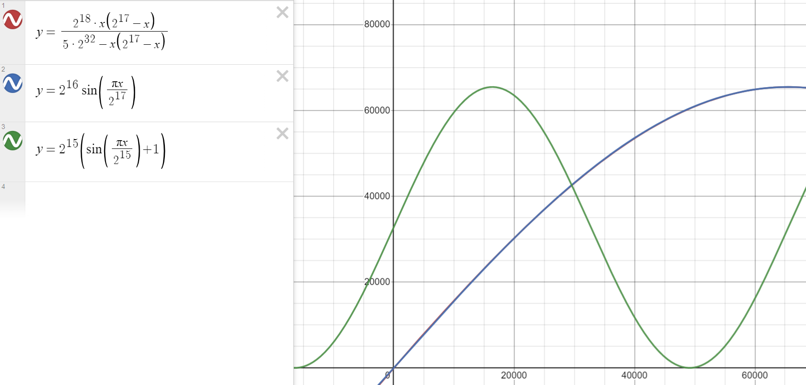
For converting a phase input to a sine amplitude, a CORDIC block is used. An initial attempt using a polynomial approximation was tested using a cocotb testbench, similarly to the final CORDIC module as explained in the testing section, Phase to sine amplitude conversion. This resulted in an accurate amplitude output, and a graph using the Desmos graphing calculator is shown in Figure x.y, where the polynomial approximation is shown in red and overlaps the reference sine wave in blue. The green line shows the final expected output from the saw2sin module. Synthesis of this polynomial approximation block resulted in 191% utilisation of the TRELLIS_COMB blocks, causing placement to fail.
[Figure: Polynomial approximation of sine wave]
Instead, a CORDIC SystemVerilog module was built while following a ZipCPU blog post on Using a CORDIC to calculate sines and cosines in an FPGA for explanations on the ideas behind the CORDIC algorithm. The CORDIC module was built to use 16 bit inputs and outputs, and the phase input represents a range of 0° - 90°. The cordic SystemVerilog module was then instantiated within the saw2sin module where it is used to recreate a full cycle of the sin wave.
Initial testing of the CORDIC module revealed that the algorithm was not accurate at extreme input values. For very small phase input values, the resulting values were too large, and for very large phase input values, the resulting values sometimes decreased as the phase increased. The issue at large phase input values was worked around by outputting a maximum output value if the input phase was above a certain threshold, 65508 in this case, as this matched the reference Python function. The issue at small phase input values was worked around by implementing a small angle approximation, where the output value is equal to 1.5x the input value for inputs below 32. The value of 1.5 was used for simplicity in implementation due to needing one right shift and one addition. The resulting CORDIC module performed much better and is the version tested in the testing section, Phase to sine amplitude conversion, including adjustments to further improve accuracy and reduce error.
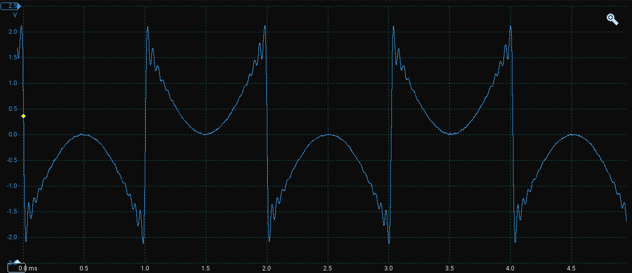
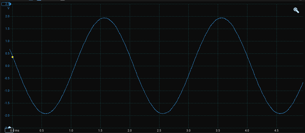
This completed saw2sin block now output a full sine wave, however the output was in the range of 0 to 65535 but the PCM1780 DAC uses signed values in the range -32768 to 32767. The effect of this is seen in Figure x.y where the resulting wave is discontinuous. To fix this, the MSB of the saw2sin amplitude output was inverted, as this is equivalent to adding half the maximum value, and the resulting audio output is shown in Figure x.z.
[Figure: Unsigned sine wave output]
[Figure: Signed sine wave output]
During testing, glitches in the output wave were discovered. These glitches were likely caused by the long critical path due to the combinatorial cordic module, so the output was changed to a registered output and the output sampled after multiple cycles. This is discussed further in the testing section, CORDIC Propagation Delay
In addition to using the value of the CORDIC module after multiple cycles, the design was to be expanded to multiple simultaneous oscillators, however instantiating a CORDIC module for each oscillator would result in wasted logic as the modules would remain unused for most cycles out of the 1000 cycles available per 48kHz sample when running at 48MHz.
To make better use of available resources, a single CORDIC module was instantiated and each phase to amplitude conversion done sequentially, in a basic form of time division multiplexing. The low 2 bits of a 48MHz counter were used to load the next phase value at step 0 and capture the resulting amplitude at step 3.
Combining Oscillators
The final stage of generating audio samples involves combining the samples from each individual oscillator into a single sample. As a single oscillator already has the maximum amplitude, the individual samples are sign extended to 24 bits before being summed into a single sample. To maintain a more consistent volume, the final sample is also shifted to the right to keep the maximum amplitude within the range of a 16 bit signed value.
The amount to shift by is calculated as the logarithm base 2 of the number of currently active oscillators minus one, so one oscillator is unaffected, two are halved and three or four are divided by four. The resulting sample will have a maximum amplitude that is between 0.5 and 1 times the maximum amplitude of a single oscillator, depending on the number of active oscillators. The SystemVerilog code for combining the individual samples is shown in Listing x.y.
[Listing: Combining individual oscillator samples]
// Add up sign extended samples
always_comb samples_long[0] = {{8{samples[0][15]}}, samples[0]};
for (genvar i = 1; i < 64; i++) begin: l_gen_sample_long
  always_comb samples_long[i] = samples_long[i-1] + {{8{samples[i][15]}}, samples[i]};
end

// Count number of active oscillators
always_comb waves_count[0] = (phase[0] != 16'd0);
for (genvar i = 1; i < 64; i++) begin: l_gen_waves_count
  always_comb waves_count[i] = waves_count[i-1] + (phase[i] != 16'd0);
end

always_comb wv_cnt_1 = waves_count[63] - 1; // Subtract 1 from wave count

always_comb shift = /* logic to calculate shift amount */;

// Shift output sample right to get normalised output
always_ff @(posedge i_clk48) samples_sum <= samples_long[63] >> shift;

always_comb o_sample = samples_sum[15:0];    // Truncate output to 16 bits
Transferring samples across clock domains
After the signed 16 bit samples have been generated, they must be transferred from the 48MHz system clock domain to the 36.864MHz DAC clock domain. Table x.y shows Table 1 from the PCM1780 [datasheet], where a sampling frequency of 48kHz allows for the following DAC system clock frequencies: 6.144MHz, 9.216MHz, 12.288MHz, 18.432MHz, 24.576MHz, 36.864MHz. Of these, 36.864MHz allows for the greatest number of cycles per sample increasing the precision of the DAC driver SystemVerilog module, at 768 cycles per sample. The DAC system clock is generated by a PLL primitive block provided by the Lattice ECP5 FPGA, which is configured to use the 48MHz system clock as the input clock, and the 36.864MHz DAC system clock as the output clock.
- TODO: fix table formatting
[Table: PCM1780 - Table 1. System Clock Frequencies for Common Audio Sampling Frequencies]
| Sampling Frequency (kHz) | System | Clock | Frequency | (MHz) | |||
|---|---|---|---|---|---|---|---|
| - | 128 fS | 192 fS | 256 fS | 384 fS | 512 fS | 768 fS | 1152 fS |
| 8 | 1.024 | 1.536 | 2.048 | 3.072 | 4.096 | 6.144 | 9.216 |
| 16 | 2.048 | 3.072 | 4.096 | 6.144 | 8.192 | 12.288 | 18.432 |
| 32 | 4.096 | 6.144 | 8.192 | 12.288 | 16.384 | 24.576 | 36.864 |
| 44.1 | 5.6448 | 8.4672 | 11.2896 | 16.9344 | 22.5792 | 33.8688 | – |
| 48 | 6.144 | 9.216 | 12.288 | 18.432 | 24.576 | 36.864 | – |
| 88.2 | 11.2896 | 16.9344 | 22.5792 | 33.8688 | – | – | – |
| 96 | 12.288 | 18.432 | 24.576 | 36.864 | – | – | – |
| 192 | 24.576 | 36.864 | – | – | – | – | – |
Transferring the samples is achieved using an Asynchronous FIFO where the read and write ports can be accessed from different clock domains. LiteX provides modules called AsyncFIFO and ClockDomainCrossing, however both require a layout parameter and no documentation is present for the format of this parameter so these modules were not used. An initial attempt was also made to design an Asynchronous FIFO from scratch following a ZipCPU Blog Post on Crossing clock domains with an Asynchronous FIFO however further research through the source files of the LiteX project revealed the Migen AsyncFIFO module. This module is derived from a _FIFOInterface class alongside documentation of the signals that are available and their expected connections to other modules.
The Migen AsyncFIFO module uses grey counters to keep track of the read and write pointers within the FIFO, preventing single bit flips from causing large glitches in the pointer values as they cross between the read and write port clock domains. In practice, the FIFO will be written to and read from at 48kHz from both clock domains, with large pauses between each sample from the perspective of both clock domains. In addition, the LiteX report states the frequency of the DAC clock domain is likely to be closer to 36.92MHz which means the FIFO will be read more often than it is filled, and should never reach the full state nor cause the sample generation to stall. The excerpt from the LiteX report is shown in Listing x.y, where the DAC system clock output is clko2 and the clko0 and clko1 outputs drive half and double system frequency clocks used for required primitive modules.
[Listing: LiteX report excerpt showing DAC clock frequency]
INFO:ECP5PLL:Config:
clko1_freq : 24.00MHz
clko1_div  : 20
clko1_phase: 0.00°
clko0_freq : 96.00MHz
clko0_div  : 5
clko0_phase: 0.00°
clko2_freq : 36.92MHz
clko2_div  : 13
clko2_phase: 0.00°
vco        : 480.00MHz
Driving the DAC (PCM1780)
The PCM1780 has a 3 wire audio interface, consisting of a bit clock, a left-right clock, and a data line. The bit clock indicates when the data line should be sampled for each bit, as the value of the data line is updated on the falling edge of the bit clock. For the default left-justified data format, left-right clock high indicates the current data is for the left channel and low indicates the current data is for the right channel. The data is sent MSB first, aligned to the falling or rising edge of the left-right clock and falling edge of the bit clock. Figure x.y in the background PCM1780 section shows the timing diagram for the default left-justified data format.
In this project, the bit clock is driven at 48 times the sampling frequency or equivalently 1/16 times the DAC system clock of 36.864MHz giving a frequency of 2.304MHz and is generated using a clock divider from the DAC system clock. This allows for 48 bits to be transferred in each period of the 48kHz left-right clock, or 24 bit left and right channel samples. In this project, the low 8 bits are left as 0s to extend the 16 bit samples from the wave generator, however the wave generator can be updated to generate 24 bit samples if required. Verification of the DAC driver was performed using the LiteScope Analyzer, which is detailed in the next section.
The PCM1780 mode bus is driven from the dacAttenuation SystemVerilog module as attenuation was identified as the only setting that may need to be user-adjustable. This module operates in the main 48MHz clock domain and divides the incoming clock by 8 to produce a 6MHz clock, which is below the 10MHz limit specified in the PCM1780 datasheet. Two shift registers are used to drive the chip select and data pins, shifting out a new value on each falling edge of the 6MHz clock signal. These shift registers are reloaded when an input valid signal is high, detected by creating a buffer register to hold the signal high for long enough to be detected in the slower 6MHz clock domain. An excerpt of the data shift register is shown in Listing x.y.
[Listing: Excerpt of the dacAttenuation data shift register]
logic [34:0] data;
always_ff @(negedge o_clock) // Update DATA on falling edge of CLOCK
  if (!i_rst48_n)    {o_data, data} <= 36'h000000000;
  else if (valid[7]) {o_data, data} <= {8'd16, volume, 2'd0, 8'd17, volume, 2'd0};
  else               {o_data, data} <= {data, 1'b0};
Testing of the design with both the dacDriver and dacAttenuation SystemVerilog modules instantiated in the top level design resulted in the design failing to boot. When either module is instantiated without the other, the design appears to boot correctly, however debugging the design when both modules are present is difficult as the LiteScope Analyzer does not function when the design fails to boot. After discussing the issue with the project supervisor, it was decided that the dacAttenuation module can be removed from the design at this stage as it is not required for a Proof-of-Concept demonstration.
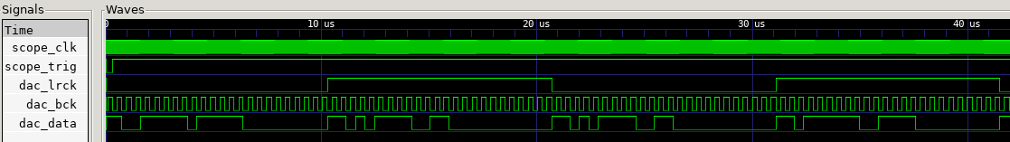
Using LiteScope Analyzer
The LiteScope Analyzer module is added to the design at the end of the BaseSoC class in make.py in the main system clock domain. The memory depth is calculated using the length of the signals being captured to prevent going over the available DP16KD memory blocks as this results in placement failing after elaboration and synthesis has already run.
LiteScope Analyzer captures every signal on each clock rising edge of the clock domain it is instantiated in. For signals that change less often than every cycle, this results in a large number of redundant samples being captured. The samplerate variable is only used in writing the analyzer.csv file and does not affect the actual sample rate of the module. A custom version of the module was created with a clock divider on the clock input to reduce the sample rate however this modification caused the design to fail to boot even when using the LiteX primitive Counter block and so the original module was used. The memory limitation was worked around by reducing the signals captured to the minimum needed for debugging or testing logic at a higher frequency before slowing it down to the intended frequency after testing.
The module is also connected to a second Wishbone UART module as a separate connection is needed to download the captured waveform data from the FPGA to the host computer for viewing. Two unused external pins are used as RX and TX pins for this UART module and connected to an FTDI232 USB to serial converter. The baudrate is also increased to 921600 baud to increase the download speed of the waveform data, which is stored in a .vcd file. Listing x.y shows the LiteScopeAnalyzer instance including defining the signals to be captured, the capture memory depth and a CSV file containing information about the module and signals to be captured.
[Listing: LiteScope Analyzer instance in make.py]
self.add_uartbone(name="debug_uart", baudrate=921600)
from litescope import LiteScopeAnalyzer
signals = [
    self.audio.dac_lrck,
    self.audio.dac_bck,
    self.audio.dac_data,
    # ... other signals to capture
]
from math import ceil, floor
analyzer_depth = floor(190_000 / ((ceil(sum([s.nbits for s in signals]) / 16)) * 16))
self.submodules.analyzer = LiteScopeAnalyzer(
    analyzer_signals,
    depth        = analyzer_depth,
    clock_domain = "sys",
    samplerate   = sys_clk_freq,
    csr_csv      = "analyzer.csv",
)
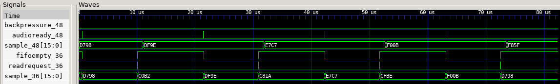
The LiteScope Analyzer instance is then accessed from the host machine using the litex_server command to start a TCP server that connects to the UART converter, and the litescope_cli command to connect to the TCP server, select trigger signals/values, and dump the received waveform data to a VCD file. The created VCD file can be viewed using programs such as GTKWave. LiteScope Analyzer was used to verify the correct operation of the AsyncFIFO and dacDriver modules. Testing the AsyncFIFO module involved checking the correct transfer of values across the clock domain crossing as well as the assertion of the back-pressure and ready flag signals. Figure x.y shows the waveform VCD as viewed in GTKWave, with the LiteScope Analyzer sampling at 48MHz.
[Figure: GTKWave screenshot of AsyncFIFO waveform]
A similar process was used in verifying the 3 signal outputs of the dacDriver module. The waveform was captured starting with a rising edge of the left-right clock, and the resulting signals compared to the expected values from the datasheet, as seen in Figure x.y from the DAC section. Figure x.z shows the waveform VCD as viewed in GTKWave, with the LiteScope Analyzer sampling at 48MHz.
[Figure: GTKWave screenshot of DAC driver waveform]
Receiving CAN Frames
A CAN receiver is required within the FPGA fabric to handle ACK signal generation and act as an interface between the CPU within the SoC and the external ATA6561 CAN Transceiver. The can SystemVerilog module contains logic for filtering of received CAN frames by ID and generation of ACK bits for accepted CAN frames.
The LiteX CanReceiver module contains two 11 bit CSRStorage fields, can_id and id_mask, shown in Listing x.y. These fields can be set from the CPU via the CSR bus and allow software to set the filter ID and mask. For every incoming CAN frame, the ID in the received frame is compared to the can_id value, and as long as all bits match where the respective id_mask bit is 1, the id_match flag is driven high. The can_id reset value of 0x123 is used to match the Embedded Systems module coursework, and the id_mask reset value of 0x7FF means only CAN frames with an ID of 0x123 will be acknowledged and stored by the module.
[Listing: CanReceiver CSRStorage fields]
self.can_id = CSRStorage(size = 11, reset = 0x123, description = "CAN ID filter")
self.id_mask = CSRStorage(size = 11, reset = 0x7FF, description = "Mask for CAN ID")
An internal counter that is incremented at 48MHz keeps track of the current bit time, where each CAN bit is expected to last for 384 cycles at 48MHz. Bits are sampled and added to the internal shift register on the rising edge of the system clock at 75% of the bit time, when the internal counter is at 287. The internal counter is reset to 0 when the current value is 383 or when a recessive to dominant (1 to 0) transition is detected on the CAN bus, maintaining synchronisation with the CAN bus and other devices.
A counter is used to keep track of the number of consecutive bits of the same polarity, being reset to 0 if the previous and current bit differ or if the counter has reached 4 indicating 5 consecutive bits of the same polarity. When the counter has reached 4, the next bit is not shifted into the internal shift register as it is a stuffed bit as discussed in the CAN Bus section.
A CAN Frame has been correctly received when the masked received ID and can_id match, the data length code is 8 and the required bits for ID extension, remote request and reserved bits are all 0. These conditions are AND'd together to produce a msg_valid flag. When the msg_valid flag is active, the received frame ID and data are stored in internal registers that are connected to CSRStatus fields, allowing the CPU to read the received frame ID and data. This flag also results in the ACK bit being sent, by driving the TX signal low to the dominant state for one bit time.
When the msg_valid flag is active, an output pin connected to an EventSourcePulse object is driven high for 1 cycle at 48MHz. This event source is connected to an EventManager which is connected to the CPU interrupt bus, creating a hardware interrupt that can be handled in an Interrupt Service Routine to copy the CAN frame ID and data into CPU memory. This interrupt logic is created in the canReceiver.py module, and an excerpt of the code showing the interrupt logic is in Listing x.y. Interrupt handling in LiteX is discussed in more detail in the interrupts section.
[Listing: canReceiver.py excerpt showing interrupts]
self.submodules.ev = EventManager()
self.ev.frame = EventSourcePulse(description = "CAN frame received, sets pending bit")
self.ev.finalize()
self.comb += self.ev.frame.trigger.eq(self.rcv_pulse)
In the interest of a quicker working proof of concept design, the can module matches values hard-coded into the ES-CAN library provided in the Embedded Systems module coursework. The DLC (Data Length Code) of CAN frames is expected to always be 8 bytes, so the DLC value is not exposed to the CPU and frames with less than 8 bytes are not acknowledged or stored. The can module can be extended to provide the received DLC value to the CPU via a CSRStatus field. The can module also does not check the CRC bits of the received frame, as bit flip errors are highly unlikely due to the short length of the CAN connection and the use of low-speed CAN. A crc_match signal is currently driven constant high but provides a location for CRC checking to be implemented in the future.
Helper functions are provided in a can library to allow students to more easily read the CSRStatus fields from the CPU. The library is discussed in more detail in the software section. The demo program includes a can_read function which continually reads the latest received CAN frame ID and data and prints it to the UART console. This function was used alongside a PicoScope to verify that the CAN frames sent from a StackSynth module are correctly acknowledged and received from the C++ demo program. This testing is detailed in the testing section.
Controlling the design from software
A large factor in the usability of the project deliverables is the ease of use of the specialised hardware from software, including student-written code running on the embedded CPU. Libraries containing helper functions are located in the demo folder of the repository and provide easier access to the registers needed to access the CAN receiver and wave generator blocks.
The demo software also includes functions from testing throughout the project, built upon functions from the auto-generated csr.h header file. These functions are wrapped in #ifdef blocks so they are only included in the compiled binary when the relevant modules are instantiated within the gateware. For example, led_cmd() and leds_cmd() set the colour of the OrangeCrab RGB LED to a user-provided value or specific values in a test pattern respectively.
The audio helper library contains functions for setting the waveform and target frequency of a specific oscillator and provides enumeration values matching the available waveforms and frequencies of notes in a range of octaves which are detected and used in editor suggestions. The helper function implementations satisfy the logic requirement of the oscillator index being set before the waveform or target frequency is set, as the write strobe signal is used as an indicator for the logic to capture the new values. The key C++ function signatures are shown in Listing x.y.
[Listing: audio.h function signatures]
void set_wave(uint32_t osc, uint32_t wave);
void set_freq(uint32_t osc, uint32_t freq);
void audio(uint32_t osc, uint32_t wave, uint32_t freq);
The can helper library contains a C++ struct definition for the CAN frame ID and data, which is used as the return type for the can_read() function and functions for reading and writing the CAN filter ID and mask. An example implementation of the CAN receiver interrupt handler and initialisation function is also provided, where the interrupt is reset and enabled and the received CAN frame is output to the serial console above the current prompt.
This interrupt handler, explained in further detail in the next section, is implemented for a software interrupt and is called from a polling interrupt service routine in the demo, as the PicoRV32 CPU does not support external hardware interrupts. The VexRiscV CPU was not used for testing the interrupt handler as this requires an interrupt handler to be registered and the documentation did not cover the software side of using hardware interrupts. The key C++ struct and function signatures are shown in Listing x.z.
[Listing: can.h function signatures]
struct can_frame {
  uint16_t id;
  uint8_t data[8];
};
uint32_t can_id_read(void);
void can_id_write(uint32_t value);
uint32_t can_mask_read(void);
void can_mask_write(uint32_t value);
can_frame can_read(void);
void can_isr(void);
void can_init(void);
Interrupts and Scheduling
In an embedded system, interrupts are a vital part of a scheduling system, allowing for higher priority tasks to be executed when required. The VexRiscV CPU supports hardware interrupts from external logic such as the canReceiver module, however documentation for software to handle these interrupts is limited.
For this section, the PicoRV32 CPU was used as external interrupts do not cause the CPU to jump to an interrupt handler and interrupts must be manually checked and handled, allowing for easier implementation of a Proof-of-Concept interrupt handler. The PicoRV32 CPU is not used in the remainder of this project as the performance is lower than the VexRiscV CPU at 0.516 DMIPS/MHzgh compared to 1.44 DMIPS/MHzgh as reported in the respective documentation.
Interrupts in a LiteX module are created by adding an EventManager which automates connection to the main interrupt bus and accepts three types of events as inputs. An EventSourcePulse triggers on a pulse and stays asserted after the trigger is de-asserted. The event is only cleared when acknowledged by software.
An EventSourceProcess triggers on either a rising or falling edge of a signal and is used to monitor the status of a signal and generate an interrupt on a change. The event is cleared when acknowledged by software. Finally, an EventSourceLevel contains the current status of an event and must be set and cleared by external logic, such as a design that keeps asserting an interrupt until the interrupt cause is cleared.
The EventManager module has an irq output indicating when an enabled interrupt is pending, a status CSR indicating the current level of an event source, a pending CSR indicating which interrupts have been triggered and not yet acknowledged and an enable CSR indicating which interrupts are active.
Following the addition of an EventManager and EventSourcePulse to the canReceiver module, an interrupt service routine is used to check for pending interrupts and handle the respective ISRs for each interrupt. Listing x.y shows the can_init() function provided in the demo can library, where the can IRQ is enabled, the specific interrupt source is enabled within the Event Manager, and a debug message is printed to the serial console.
[Listing: can_init() function]
void can_init(void) {
  irq_setmask(irq_getmask() | (1 << CAN_INTERRUPT));
  can_ev_enable_frame_write(1);
  printf("CAN INIT\n");
}
Listing x.z shows the can_isr() function provided in the demo can library. The ISR first clears the pending event in the Event Manager, then reads the last received CAN frame. For debugging purposes, the CAN frame is printed to the serial console and the prompt and current input buffer restored. Finally, the CAN frame interrupt is re-enabled in the Event Manager. The ISR also changes the current LED colour to make it clearer when the ISR has run. The code to change the LED colour and print to the serial console is not shown in the listing for brevity.
[Listing: can_isr() function]
void can_isr(void) {
  can_ev_pending_frame_write(1);
  // Update LED to make it clear that the ISR has run...
  can_frame frame = can_read();
  // Print CAN frame to serial console...
  // Reprint prompt and current input buffer...
  can_ev_enable_frame_write(1);
}
Along with the LiteX built-in Timer module, interrupts can be used to create hardware timers. This is especially beneficial for supporting real-time operating systems such as FreeRTOS, where timers can be used to create initiation triggers for tasks and interrupts are used for unpredictable events such as receiving CAN frames as in the Embedded Systems coursework. This is explained in further detail in the further work section.
FPGA Utilisation
As this project uses an FPGA, a major limitation on the performance of the design is the available resources. In the output of the nextpnr placement stage, there is a device utilisation report which shows the number of each type of logic element and primitive block used. Table x.y shows the FPGA utilisation report, and an excerpt of the logs containing the original report is included in Appendix x.y.
[Table: FPGA utilisation report]
| Logic Element | Used | Total | Utilisation % |
|---|---|---|---|
| TRELLIS_IO | 74 | 197 | 37 |
| DCCA | 8 | 56 | 14 |
| DP16KD | 49 | 56 | 87 |
| MULT18X18D | 2 | 28 | 7 |
| ALU54B | 0 | 14 | 0 |
| EHXPLLL | 2 | 2 | 100 |
| EXTREFB | 0 | 1 | 0 |
| DCUA | 0 | 1 | 0 |
| PCSCLKDIV | 0 | 2 | 0 |
| IOLOGIC | 49 | 128 | 38 |
| SIOLOGIC | 0 | 69 | 0 |
| GSR | 0 | 1 | 0 |
| JTAGG | 0 | 1 | 0 |
| OSCG | 0 | 1 | 0 |
| SEDGA | 0 | 1 | 0 |
| DTR | 0 | 1 | 0 |
| USRMCLK | 0 | 1 | 0 |
| CLKDIVF | 1 | 4 | 25 |
| ECLKSYNCB | 1 | 10 | 10 |
| DLLDELD | 0 | 8 | 0 |
| DDRDLL | 1 | 4 | 25 |
| DQSBUFM | 2 | 8 | 25 |
| TRELLIS_ECLKBUF | 3 | 8 | 37 |
| ECLKBRIDGECS | 1 | 2 | 50 |
| DCSC | 0 | 2 | 0 |
| TRELLIS_FF | 7790 | 24288 | 32 |
| TRELLIS_COMB | 24126 | 24288 | 99 |
| TRELLIS_RAMW | 95 | 3036 | 3 |
- TODO: Move to appendix
[Listing: FPGA utilisation report]
Info: Device utilisation:
Info:             TRELLIS_IO:    74/  197    37%
Info:                   DCCA:     8/   56    14%
Info:                 DP16KD:    49/   56    87%
Info:             MULT18X18D:     2/   28     7%
Info:                 ALU54B:     0/   14     0%
Info:                EHXPLLL:     2/    2   100%
Info:                EXTREFB:     0/    1     0%
Info:                   DCUA:     0/    1     0%
Info:              PCSCLKDIV:     0/    2     0%
Info:                IOLOGIC:    49/  128    38%
Info:               SIOLOGIC:     0/   69     0%
Info:                    GSR:     0/    1     0%
Info:                  JTAGG:     0/    1     0%
Info:                   OSCG:     0/    1     0%
Info:                  SEDGA:     0/    1     0%
Info:                    DTR:     0/    1     0%
Info:                USRMCLK:     0/    1     0%
Info:                CLKDIVF:     1/    4    25%
Info:              ECLKSYNCB:     1/   10    10%
Info:                DLLDELD:     0/    8     0%
Info:                 DDRDLL:     1/    4    25%
Info:                DQSBUFM:     2/    8    25%
Info:        TRELLIS_ECLKBUF:     3/    8    37%
Info:           ECLKBRIDGECS:     1/    2    50%
Info:                   DCSC:     0/    2     0%
Info:             TRELLIS_FF:  7790/24288    32%
Info:           TRELLIS_COMB: 24126/24288    99%
Info:           TRELLIS_RAMW:    95/ 3036     3%
Lines of importance from Table x.y include:
- DP16KD: dual-port RAM blocks, used in the CPU and the sample storage of the LiteScope Analyzer
- 49/56 used: the memory of the Analyzer is limited due to this, but the design is unlikely to require more than are currently used
- MULT18X18D: 18x18 multipliers, used in the CPU and for phase-step calculation in the
cordicblock- 2/28 used: a previous iteration of the
cordicblock where all phase-steps were calculated combinatorially in parallel resulted in 65/28 multipliers
- 2/28 used: a previous iteration of the
- EHXPLLL: Phase-Locked Loop, used for generating the 48MHz and other clock signals required in the design
- 2/2 used: the design already uses both available PLLs, one for the USB PHY and one for the remainder of the design, where the DAC clock output was added
- TRELLIS_FF: DFF (D-type flip-flop) logic elements, used to store signals between clock cycles
- 7790/24288 used: the design current;y uses 32% of the available resource so there is room for expansion
- TRELLIS_COMB: combinational logic elements, used for all logic in the design between clocked elements
- 24126/24288 used: determines the amount of logic that can be implemented in the design, this is the limiting factor to adding more features to the design
The breakdown of TRELLIS_COMB usage is helpful in identifying blocks that could be optimised, however the version of nextpnr provided as part of Project Trellis does not include the GUI and the command-line program does not expose per module utilization reports. As a comparison, the LUT4 utilisation has been used as an approximation of the logic utilisation of each module, as provided in the synthesis report by Yosys, shown in Table x.y. The table shows that the cordic module is small relative to the PicoRV32 CPU, however the genWave module uses a large amount of logic and is likely a target for future optimisation.
[Table: TRELLIS_COMB breakdown]
| Module | LUT4 Usage |
|---|---|
| gsd_orangecrab | 15543 |
| picorv32 | 3027 |
| can | 139 |
| dacDriver | 62 |
| genWave | 8874 |
| saw2sin | 61 |
| cordic | 1066 |
For further additions to the design, an increase in unused logic will be required. The OrangeCrab model could be swapped from the LFE5U-25F model to the LFE5U-85F, which has 84k LUTs, 3744Kb of embedded RAM and 669Kb of distributed RAM, however this would lead to increased per-board cost of producing the StackSynth FPGA Extension boards.
Alternatively, the number of logic elements used in the design could be reduced. One method would be to reduce the number of available oscillators, reducing the logic and storage for calculating phase-steps and combining samples, however the logic used to convert phase to samples is shared between all of the oscillators so the decrease in logic element usage is likely to be small. Another method would be to replace the VexRiscV and PicoRV32 CPUs used in this design with a smaller CPU at the expense of performance. The viability of these options is not known, and is left as future work.
Testing and Results
This section discusses the testing of individual blocks within the overall design, and the tools used to verify correct operation.
Phase to sine amplitude conversion
One area with a noticeable impact on performance is the phase to sine amplitude conversion of samples within the cordic and saw2sin SystemVerilog modules, as incorrect amplitude values can result in audible glitches in the waveform output at the 3.5mm headphone port. The cordic module was first checked as a standalone module, and then integrated into the saw2sin module and exhaustively tested at each input value as the output amplitude only depends on the input phase and waveform selections, with no internal state between input values.
This testing was automated using cocotb, a Python-based verification framework for SystemVerilog and VHDL designs, and the repository containing the modules and testbench is available on GitHub. The Python testbench defines the timing and values of the inputs and checks the output value against the reference, however simulation is handled by an external simulator. In this module, only two-state simulation is needed as unknown and high impedance values are not used so Verilator is used as the simulator, as simulations are much faster than other simulators while maintaining cycle accuracy. If exact timing is required, using another simulator may be more appropriate as support for timing directives is limited in Verilator.
The testbench is a function which loops through the 65536 possible input values, and for each value sets the input phase i_saw and reads the output amplitude o_sin. The output amplitude is then compared to the expected value e_sin, which is calculated using the sin() function in Python and the error added to the total recorded error. Any errors above 2 from the expected float value are logged and after the loop completes, the average error per input is displayed. The Python testbench is shown in Listing x.y and can be run by cloning or downloading the repository and running make in the root directory.
[Listing: Python cocotb testbench for saw2sin module]
# import statements...

@cocotb.test() # cocotb test decorator
async def test_new_cordic(dut):
    await cocotb.start(Clock(dut.i_clk, 10, units='ps').start()) # start clock coroutine
    diff = 0                                              # total error
    for cycle in range(0, 65536):                         # loop through input values
        dut.i_saw.value = cycle                           # set the input phase
        await Timer(20, units='ps')                       # wait so output can settle
        e_sin = 32768 * (sin((cycle * pi) / (2**15)) + 1) # calculate expected output
        error = float(dut.o_sin.value) - e_sin            # calculate error
        if abs(error) > 2:                                # log any errors above 2
            dut._log.info()                               #   error message...
        diff += abs(error)                                # add error to the total

    dut._log.info("Testbench finished, average error %f" % (diff / 65536))
Using the testbench in Listing x.y, the accuracy of the saw2sin module was improved by adjusting the bit offsets of the amplitude output for the four quadrants of the sine wave output. The final accuracy achieved was an average error of 0.455326 per input value meaning the integer output of the saw2sin value is within 1 of the expected value on average. Listing x.z shows the an excerpt of the saw2sin SystemVerilog module where the offsets can be adjusted for each of the four quadrants of the sine wave.
[Listing: SystemVerilog saw2sin module, excerpt of adjusting amplitude offsets]
// Signals for `reverse` and `invert` indicate the quadrant of the sine wave

logic [16:0] sin;
always_ff @(posedge i_clk) sin <= reverse
  ? (invert ? ~{1'b1, qsin[15:0]}          // Reverse, Invert: 270-360°
            : {1'b1, qsin[15:0]} + 17'd1)  // Reverse, Normal: 90-180°
  : (invert ? ~{1'b1, qsin[15:0]} + 17'd2  // Normal, Invert: 180-270°
            : {1'b1, qsin[15:0]} + 17'd0); // Normal, Normal: 0-90°

always_comb o_sin = sin[16:1]; // Remove extra bit used for offsets
CORDIC propagation delay
In the implementation of the genWave SystemVerilog module, the cordic module is used to convert a phase value to a sine amplitude, however when viewing the output of the PCM1780 using a PicoScope, visible glitches were observed in the waveform output. A screenshot of the PicoScope software is shown in Figure x.y, where the glitch in the output can be seen, and Figure x.y2, where a mask is used to show glitches from multiple captures at once. The glitches primarily occur near when the wave changes sign, or when the MSB of the amplitude changes. The expected cause of this glitch was propagation delay differences between the bits of the amplitude output. To mitigate this, the combinatorial output of the cordic module was replaced with a synchronous output by changing the always_comb statement to an always_ff @(posedge i_clk). This change removed the glitches from the waveform output, as shown in Figure x.z.
[Figure: PicoScope screenshot of glitch in waveform output]
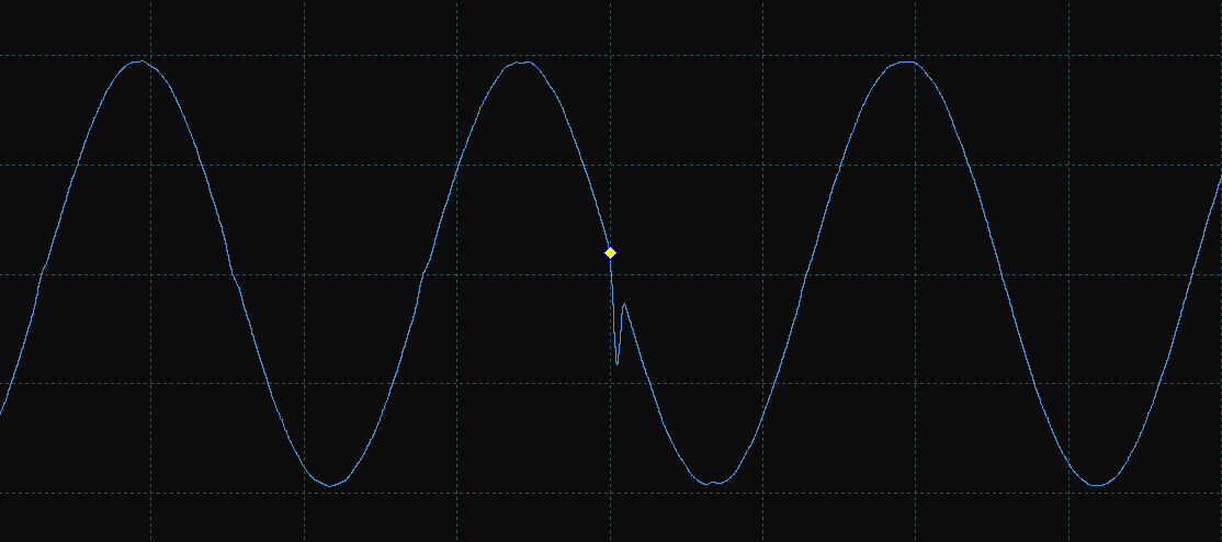
[Figure: PicoScope screenshot of masked glitches in waveform output]
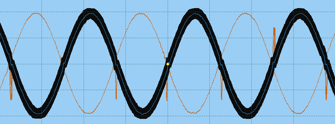
[Figure: PicoScope screenshot of waveform output without glitches]
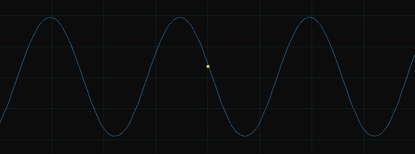
As the cordic module was no longer combinatorial, the genWave module would need to sample or capture the output once it is stable. The propagation delay of the cordic module was measured by using a counter to iterate through all 65536 input values, incrementing every 8 cycles, and then connecting the i_saw and o_sin signals to the LiteScope Analyzer, checking the time taken for the output to stabilise. The cocotb testbench is available in the project files at modules/testPropagation.py, and resulting waveform VCD file at notes/testPropTiming.vcd.
A screenshot of the VCD file in GTKWave is included in Figure x.y. The propagation delay of the cordic module was measured to be 1-2 cycles at 48MHz, so the output is sampled after 3 cycles to ensure the output is stable. An excerpt of the genWave module showing the value capture after 3 cycles is shown in Listing x.z.
[Figure: GTKWave screenshot of cordic propagation delay]
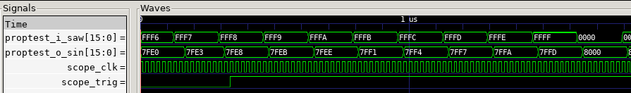
[Listing: SystemVerilog genWave module, excerpt of capturing cordic output]
// Saw amplitude captured on cycle 0
always_ff @(posedge i_clk48) if (clk_div[1:0] == 2'd0) saw <= phase[clk_div[7:2]];

// Waveform selection
always_comb // Select waveform sample based on wav_sel for current oscillator
  case (wav_sel[clk_div[7:2]])
    8'd0: sample = saw;
    8'd1: sample = square;
    8'd2: sample = triangle;
    8'd3: sample = sine;
    default: sample = saw;
  endcase

// Sample captured on cycle 3
always_ff @(posedge i_clk48) if ((clk_div[1:0] == 2'd3) && osc_valid)
  samples[clk_div[7:2]] <= sample;

// Remaining module code...
Receiving and acknowledging CAN frames
Operation of the CAN receiver module was verified by connecting the StackSynth FPGA Extension board to the main StackSynth module and sending CAN frames. A PicoScope was connected to the CANL pin of the StackSynth inter-board connector using probe A (blue) and GPIO 11 of the OrangeCrab using probe B (red). The PicoScope serial decoder was set up to decode the CAN bus signal and display the received CAN frames, including whether the communication is valid or invalid.
Figure x.y shows a screenshot of the PicoScope software, where GPIO 11 of the OrangeCrab was driven by the stuff_bit signal of the CAN receiver module and this signal matches the stuff bits indicated by the PicoScope Serial Decoder. In the figure, two CAN frames are correctly acknowledged, with both having an ID of 0x123 and data bytes of 0x5206010000000000 and 0x5206030000000000. In the Embedded Systems module, these correspond to note-down events for octave 6 note 1 or C and octave 6 note 3 or D respectively.
Figure: PicoScope screenshot of CAN bus
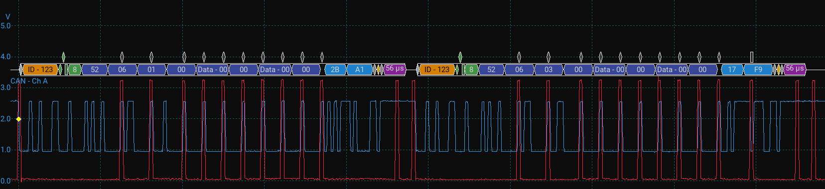
Software-interrupt detection of CAN frames
Interrupts from the CAN receiver module to the CPU were verified using the PicoRV32 CPU as this CPU does not jump to an interrupt handler when an external interrupt is received. This is helpful for testing as the documentation of the LiteX project on registering an interrupt handler is incomplete, stopping after the Event Manager is connected to the CPU interrupt port. To demonstrate that the interrupts reach the CPU, are correctly identified and handled, the demo program includes an interrupt service routine that runs in a polling manner in the main loop before the serial console input handler runs. This interrupt service routine checks if any interrupts are pending and which, and calls the respective interrupt handler.
The CAN interrupt handler, discussed in the interrupts section, is called when the CAN frame received interrupt is detected, and reads the latest received CAN frame values. The CAN frame ID and data is then printed above the current serial console input line, an excerpt from the LiteX Terminal is shown in Listing x.y. Along with printing the CAN frame values, the interrupt handler also updates the current OrangeCrab RGB LED colour. This test of functionality is a demonstration and does not have quantitative results to explain.
[Listing: CAN interrupt handler printing received CAN frame]
CAN frame    12 received, ID: 0x123, data 0x52 0x06 0x01 0x00 0x00 0x00 0x00 0x00

StackSynth> input restored here
Integration with StackSynth board
Finally, the StackSynth FPGA Extension board was tested with the StackSynth module to verify that the CAN bus communication and sample generation works, including multiple keys at once. In order to test multiple key audio output, the can_listen() command was added to the demo program. Listing x.y shows the can_listen() function, which is called when the can_listen command is entered into the LiteX Terminal.
This function keeps track of which notes are currently active and which oscillators are being used for those notes, updating the active notes and oscillator frequencies as note down and note up events are received over the CAN bus. It does not use the interrupt handler as it is a demo of audio production however the logic could be separated into tasks as part of future work to shift to a real-time operating system such as FreeRTOS, however the helper functions in the audio and can libraries are used to simplify the code.
- TODO: move listing below to appendix
[Listing: can_listen() function]
const uint32_t freqs[85] = {/* integer frequencies for notes used by StackSynth module */};
static void can_listen_cmd() {
  for (int i = 0; i < 64; i++) { // Set all oscillators to sine wave
    set_wave(i, WAVE_SINE);
  }
  bool active_notes[85] = {0};
  uint32_t active_osc[64] = {0};
  uint32_t active_oscs = 0;
  while (true) {
    can_frame frame = can_read(); // Read CAN frame
    switch (frame.data[0]) {
      case 'P': { // Note down event
        uint32_t note = (frame.data[1] - 1) * 12 + frame.data[2];
        if (active_notes[note] || active_oscs == 64) // ALready active or all oscillators in use, ignore

        active_notes[note] = true;          // Mark note as active
        active_osc[active_oscs] = note;     // Set oscillator to note
        set_freq(active_oscs, freqs[note]); // Set oscillator frequency
        active_oscs++;
        break;
      }
      case 'R': { // Note up event
        uint32_t note = (frame.data[1] - 1) * 12 + frame.data[2];
        if (active_notes[note] == false) { // Not active, ignore
          break;
        } else if (true) {
          active_notes[note] = false; // Mark note as inactive
          active_oscs--;
          if (note == active_osc[active_oscs]) { // Note is last active
            active_osc[active_oscs] = 0;         // Clear oscillator
            set_freq(active_oscs, 0);            // Set frequency to 0
            break;
          }                                             // Note is not last active
          for (uint32_t i = 0; i <= active_oscs; i++) { // Find note
            if (note != active_osc[i]) {
              continue;
            }                                                // Note found
            uint32_t swapped_note = active_osc[active_oscs]; // Get last active note
            set_freq(i, freqs[swapped_note]);                // Set frequency to last active
            active_osc[i] = swapped_note;                    // Set oscillator to last active
            set_freq(active_oscs, 0);                        // Set last oscillator to 0
            active_osc[active_oscs] = 0;                     // Clear last active note
            goto done;                                       // Done (break only exits for loop)
          }
          break;
        }
      }
      default: { // Ignore other frames
        break;
      }
    }
  done:
    if (readchar_nonblock()) { // Check for input and exit
      getchar();
      for (int i = 0; i < 64; i++) { // Reset all oscillators
        audio(i, WAVE_SAWTOOTH, 0);
      }
      return;
    }
  }
}
C++ standard library data structures such as a set or vector are more appropriate for such a function however the libraries failed to link when testing with the GCC compiler provided by the litex_setup.py script. Another version of GCC may allow standard library structures and headers to be used. Listing x.z shows the output from GCC when attempting to compile a program with #include <vector>.
[Listing: GCC error when including vector]
/usr/riscv64-linux-gnu/include/gnu/stubs.h:8:11:
fatal error: gnu/stubs-ilp32.h: No such file or directory
    8 | # include <gnu/stubs-ilp32.h>
And finally, a measure of the performance improvement in audio quality between the StackSynth and FPGA Extension boards is the SNR (Signal-to-Noise Ratio) of the audio output as a higher SNR would result in a lower noise floor and clearer audio for the same signal amplitude. Table x.y contains the frequency, SNR and THD results for the StackSynth board and the FPGA Extension board when using a target frequency of 3520Hz (A7), each using 500 samples in the measurement. The screenshots of the PicoScope measurements are included in Appendix x.y.
The results show a small but measurable improvement in SND as well as THD, while the frequency is slightly further from the target on the FPGA. Overall the audio performance of a single oscillator is similar, however the FPGA accelerator is capable of many more oscillators simultaneously.
[Table: SNR and THD of StackSynth and FPGA Extension boards]
| Board | Frequency (Hz) | SNR (dBc) | THD (%) |
|---|---|---|---|
| StackSynth | 3520.29 | 24.48 | 2.71 |
| FPGA Extension | 3520.60 | 25.18 | 2.12 |
Evaluation
The main difficulty in this project came from the lack of documentation of specific features or modules provided by the LiteX framework, as the overall flow of building gateware and software is largely automated, however extending the default gateware with custom modules that connect to existing designs requires precise Python structures to be built in order to synthesize to the expected design. The SoC and modules developed in this project can be built upon and can act as a form of documentation of the less documented features of LiteX, such as the interconnection of modules and process of building custom software to run on the embedded CPU.
The SoC and software developed in this project allow a student to compile gateware for the OrangeCrab FPGA, write software to decode CAN frames and control the 64 available oscillators. This can be used as an extension to the current 3rd Year Embedded Systems coursework to allow for many more frequencies to be generated at once, including more complex effects such as chords from a single note press on the StackSynth module. While this project aims to be a direct extension of the existing coursework, students planning to use the OrangeCrab FPGA will need to install the LiteX framework as the upload of user software requires the LiteX Terminal, even if the gateware does not need to be compiled or re-flashed to the OrangeCrab FPGA.
Writing user software for the SoC also requires the LiteX framework to be installed, as the version of GCC that is included provides many header files that are required for the compilation of the software and the LiteX setup script automates the installation of the required version of GCC for the RISC-V CPUs used in the SoC. Other header files such as the auto-generated csr.h definitions file can be reused from this project as long as the gateware is not changed, and the provided helper function libraries build upon the defined macros and functions in the csr.h file.
Of the goals identified in the Requirements Capture section, the ability to receive CAN frames via the inter-board connector and drive multiple oscillators simultaneously from user software have been met as 64 oscillators are available. The ease of use of the custom modules is not quantitatively measurable, however the style of functions in the audio and can C++ headers aim to match the style of functions in the ES_CAN header file provided in the current Embedded Systems coursework.
The primary goal identified that has not been met in this project is the implementation of filter modules that would allow more complex sound effects to be created such as equalisation filters or distortion effects. The filter modules were omitted as the completion of the core modules and overall Proof-of-Concept design took longer than expected due to the experimentation needed in the early stages of the project to understand the LiteX framework. However, were a filter module to be implemented, it could be easily inserted in-between the sample generation module and the Asynchronous FIFO, including multiple filter blocks in series to create a pipeline of filters that affect the incoming samples sequentially. Such an implementation would scale linearly in resources as the number of filter stages is increased, however the filter logic could also be reused for multiple sample calculations to allow the number of filter stages to scale more efficiently at the cost of code complexity and timing requirements.
The current design is very high in resource utilisation when synthesised using Yosys, as discussed in the FPGA Utilisation section, and optimisations have been made to allow the design to fit within the Lattice LFE5U-25F such as shared use of modules and logic, however features such as filters and effects on a stream of samples will require extra logic either requiring further optimisation or an FPGA with more resources.
Conclusions and Further Work
This report presented the available resources and implementation of an FPGA Accelerator for the StackSynth module, allowing for many more oscillators than is possible solely in the CPU of the Nucleo L432KC microcontroller. The shared use of computational logic reduces the resource requirements of the design and allows for the use of the OrangeCrab FPGA which is small enough to fit next to the main StackSynth module. Careful timing analysis of high speed signals using LiteScope Analyzer along with the PicoScope for longer-duration signals contributed to the protocol compatible function of the canReceiver and dacDriver modules.
The main benefit of the work completed in this project is the ability to extend the current design with new modules while supporting software control of these new modules, as much of the benefit of LiteX comes from the automatic generation of pre-processor definitions and functions to ease communication with and control of external modules.
While working on the implementation of this project, possible avenues for further work were identified, specifically greater precision in target frequencies and the addition of software support for hardware interrupts to the embedded CPU.
The wave generation block currently accepts integer format values for the target frequency of each oscillator, however this restricts the precision of the selectable frequencies, especially at lower frequencies where the changes in calculated phase step are greater. The phase step calculation can be adjusted to support a fixed point format where the input target frequency value is a power of two multiple (x2^n) of the desired target frequency, and then the phase step is shifted right to compensate for the scaling. A version of the genWave module using a 24.4 bit fixed point format was implemented, however when attempting to compile software for the SoC, any use of floating point values and operations caused the compile to fail due to missing library files, so this enhancement has been left as future work. Preliminary research suggests that the picolibc setting for print and scan support may remove support for floating point values, as explained in the picolibc GitHub repository printf documentation.
With an event source and event manager, the current implementation of the can module is correctly connected to the interrupt port of the embedded CPU and generated interrupt signals when requested from the SystemVerilog module using a pulse, however the demo software does not currently include the necessary setup to handle hardware interrupts as supported by the VexRiscV CPU. The addition of hardware interrupts and an interrupt handler would allow for more flexibility in the user software and may allow for running FreeRTOS on the OrangeCrab FPGA, bringing the experience of writing software for the SoC closer to that of the existing StackSynth module. Handling of an interrupt as soon as it occurs also reduces the chances of a second interrupt occurring before the first handler has finished running, which could cause the second interrupt to be missed if of the same type or an urgent task to be delayed.
- TODO: Volume control / amplification for low impedance headphones using the DS1881E digital potentiometer and TS482 Stereo Amplifier
User Guide
- TODO: Move to appendix, and include API documentation
This project is easiest to build on a Unix-like system, eg Linux or macOS (including WSL2), but can be built on Windows though instructions may need to be adapted.
Prerequisites
More information on toolchain setup can be found on the OrangeCrab Getting Started Guide
- Python 3.6+
dfu-util(also providesdfu-suffix)- Can be installed via
sudo apt install dfu-utilon Ubuntu, more information on the project website - LibUSB drivers for Windows, or
udevrules for Linux, explained in detail on thedfu-utilproject website
- Can be installed via
- Yosys and nextpnr
- Can be installed separately, following the guide for Project Trellis
- Precompiled versions available as part of the OSS CAD Suite
- Check using
yosys -Vandnextpnr-ecp5 -V
- LiteX
- Follow the installation guide to install the LiteX packages to your environment
- Meson, Ninja and Sphinx tools using
pip3 install meson ninja sphinx - RISC-V GCC using
sudo ./litex_setup.py --gcc riscvwhich installsgcc-riscv64-linux-gnuor equivalent
If using WSL2, you will also need to install usbip in the Linux distribution and usbipd-win on Windows. The wiki is helpful for setting up WSL2 USB pass-through.
Running the Project
After downloading or cloning the repository, the remaining steps are handled by the build.sh bash script, but the stages are also explained here in case you want to run them manually or are using Windows without WSL2. (Optional) steps prompt the user for confirmation, in case you want to skip them on subsequent runs.
- (Optional) Build the Bitstream file
- Run
python3 --build --docto build the bitstream and documentation of the SoC - The built documentation is located in
build/gsd_orangecrab/doc/_build/html/ - Move / rename the bitstream to a more convenient location,
mv build/gsd_orangecrab/gateware/gsd_orangecrab.bit gsd_orangecrab.dfu - Apply the DFU suffix to the bitstream,
dfu-suffix -v 1209 -p 5af0 -a gsd_orangecrab.dfu
- Run
- (Automatic) Build the demo software, C++
- From the project root, run
BUILD_DIR=`realpath -eL build/gsd_orangecrab/` WITH_CXX=1 make -C demo - The resulting binary is located at
demo/demo.bin
- From the project root, run
- (Optional) Flash the bitstream to the OrangeCrab
- Run
dfu-util -w -D gsd_orangecrab.dfuand press the button on the OrangeCrab to enter the bootloader, flashing will begin when the bootloader is detected
- Run
- (Optional) Load the demo software over a serial connection using
litex_term- Run
litex_term --kernel {path to demo.bin} /dev/ttyACM0, then either press the button on the OrangeCrab to reboot, or typeserialbootorrebootin the LiteX terminal - On Windows, the port will be a COM port rather than a TTY, and on Unix systems, the port may be different
- Run
Bibliography
List of links in proper referencing format.
Appendix
Used as necessary. State where the code can be found online? Include / refer to all technical details needed for another person to continue development.
- Code (links to source online)
- Test data? Generated by testbench as needed
- Raw results? Generated by testbench in a deterministic manner
- Related material, eg manuals / documentation
- Sections of the DAC / CAN chip datasheet that are of particular interest